Ion beam tools have become inevitable in today's science and technology research and industrial applications. The application spans over several areas and traditionally have addressed milling, patterning, high resolution imaging and implantation, including fundamental physics research. In order to serve emerging research applications, there are efforts to develop ion beam tools that use gaseous plasmas, which can be non-toxic and therefore suitable for biomaterials and provide an option for rapid processing due to higher currents without metallic contamination. To mention a few, ion beam processing of polymer biomaterials (e.g polyurethane and silicon rubber) are becoming increasingly important for applications in artificial heart valves. The surface properties of metallic bio-materials such as titanium/titanium alloys and cobalt-chromium alloys (Co-Cr) used in orthopedic prostheses, can be improved by employing nitrogen ion beams which reduces wear and tear. For microfluidic applications sometimes network of channels are required in the micro-meter regime. As a possibility to address the above requirements, a microwave plasma based multi-element ion beam system has been developed, that can deliver ion beams of different gaseous elements (e.g. Ar, Kr, Ne, H2) with the present capability of focusing the beam down to single digit in micrometers.

Fig. 1. Digital picture of the variable gaseous plasma focused ion beam system.
The ion beams have an axial ion energy spread ~ 5 eV (shown in Fig 2) which is comparable to conventional commercially available Ga focused ion beams systems.

Fig. 2. Comparison of the ion energy distribution at the beam extraction region with standard Maxwellian (fM) and Druyvesteyn (fD) distributions having same mean energy.
Recently this system has been used to create high aspect ratio (Line width/ depth) microstructures in the range 100 - 1000, as shown in Figure. 3. Variable milling rates in the range 1 – 500 µm3/s on metallic copper substrates can be easily achieved. The abbreviated name of our institute "IITK", engraved on copper thin films including other microstructures created by the ion beams is shown in Figure 4. It is expected that the device will be able to address emerging areas in microfluidics and rapid processing of biomaterials.

Fig. 3. Variation of aspect ratio with writing speed for Ar, Kr and Ne ion beams
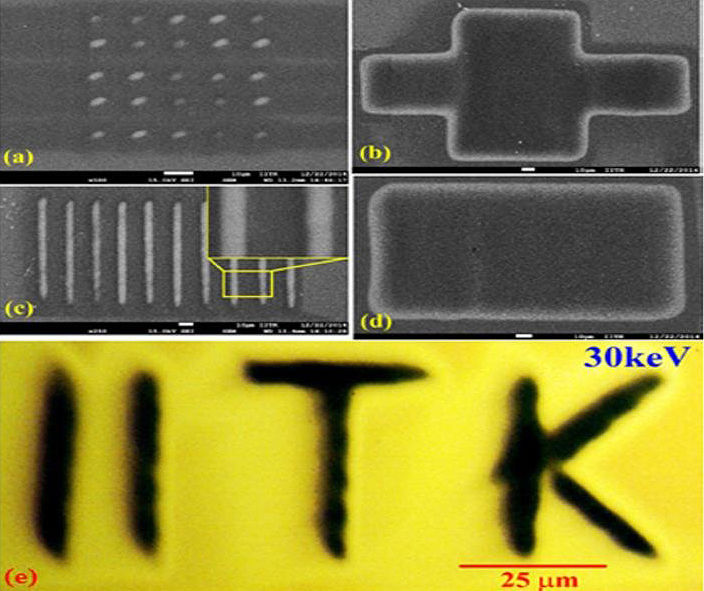
Fig. 4. Images of Ar ion beam writing on 50 nm Cu thin film. Scanning electron microscope (SEM) images of (a) 5 × 5 arrays of micro-spots created by 0.4 s irradiation, (b) cross symbol, (c) gratings of 50 /mm rulings, and (d) rectangle of 180 µm × 120 µm, written with 18 keV for the 31µm plasma electrode aperture (the white scale bar on (a)-(d) represents 10 µm). (e) Optical microscopy image of our institute's name "IITK" written with 30 keV for ther 45µm PLE aperture (the red scale bar represents 25µm).
References
-
J. V. Mathew, I. Dey and S. Bhattacharjee, Microwave Guiding and Intense Plasma Generation at Subcutoff Dimensions for Focused Ion Beams, Applied Physics Letters 91, 041503 (2007).
-
J. V. Mathew and S. Bhattacharjee, Compact Electrostatic Beam Optics for Multi Element Focused Ion Beams: Simulation and Experiments, Review of Scientific Instruments, 82, 013501 (2011).
-
Sanjeev K. Maurya, Samit Paul, Jay Kumar Shah, Sanghamitro Chatterjee, and Sudeep Bhattacharjee, Momentum transfer using variable gaseous plasma ion beams and creation of high aspect ratio microstructures, Journal of Applied Physics, 121,123302 (2017).
Research Patent
The device has been built at IIT Kanpur with support from DST and has recently received a US patent (patent no. US-9576767 issued on 21 Feb 2017).


