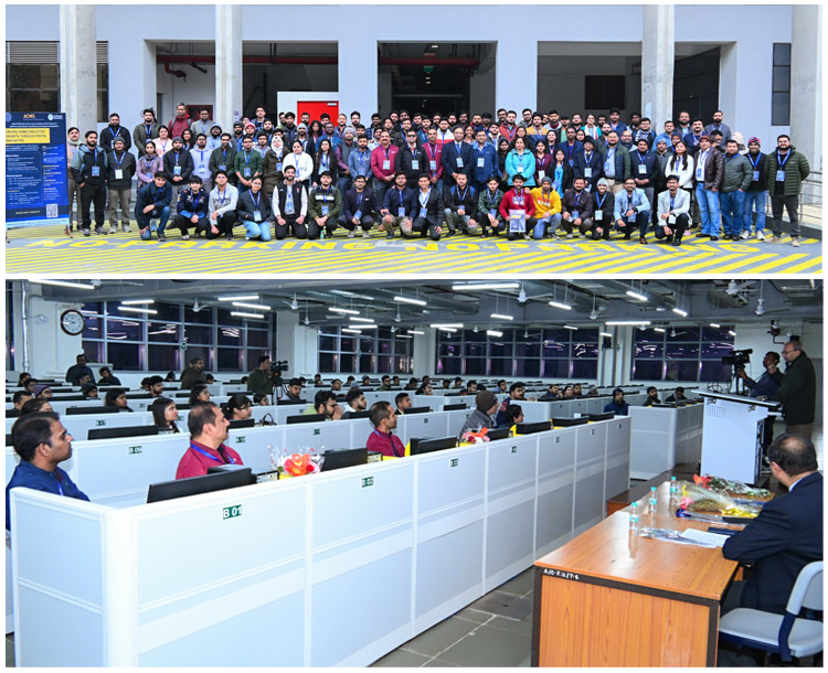
Advanced Centre for Materials Science (ACMS), IIT Kanpur, collaborated with Applied Materials India, to organize a one-day hands-on workshop titled “Driving Semiconductor Growth Through Digital innovation”
Kanpur , 11 February 2026
Source: Information and Media Outreach Cell, IIT Kanpur
Kanpur, February 11, 2026: Advanced Centre for Materials Science (ACMS), IIT Kanpur, along with Applied Materials India, organized a hands-on workshop at IIT Kanpur. In this workshop, Applied Materials showcased its foundational software framework, Applied Twin - a sophisticated digital twin solution designed to model and optimise semiconductor manufacturing equipment and processes.
Various aspects of the software framework were explained by guest speakers from Applied Materials who also guided the participants through hands-on tutorials. The participants got a chance to work on the foundational multi-physics software suite to simulate thermal chemical vapor deposition (CVD), plasma enhanced chemical vapor deposition (PECVD) and etching processes, and to see the effect of various parameters on these processes.
The software framework from Applied Materials is also being used as an educational tool at IIT Kanpur to bridge the gap between theoretical aspects of semiconductor fabrication to the real fabrication workflows at a semiconductor fab through virtualization of processes and control.
The workshop was inaugurated by Prof. Manindra Agrawal, Director of IIT Kanpur. Prof. Agrawal welcomed the participants and guests and appreciated Applied Materials' collaboration with IIT Kanpur towards skill development in semiconductor manufacturing.
The inauguration ceremony was also graced by the presence of Prof. Tarun Gupta, Dean, Research and Development, IIT Kanpur, Prof. Kantesh Balani, Head, Materials Science and Engineering, and invited faculty members from various departments.
Prof. Anish Upadhyaya (Head, ACMS) emphasized the importance of “learning by doing,” as is the tradition with many workshops on various material characterization techniques organized by ACMS.
The workshop was attended by over 120 participants, including faculty, staff, and students (UG and PG) from IIT Kanpur, HBTU Kanpur, and other places. Prof. Monica Katiyar and Prof. Anshu Gaur from the Department of Materials Science and Engineering gave introductory talks on processes involved in semiconductor chip fabrication and the role of plasma in semiconductor fabrication, which helped the participants use the simulation tools with an understanding of the processes used in chip manufacturing.
About IIT Kanpur
The Indian Institute of Technology Kanpur, established in 1959, is recognized as an Institute of National Importance by the Government of India. Renowned for excellence in science, engineering, and interdisciplinary education, IIT Kanpur spans a 1,050-acre lush green campus and comprises 20 departments, 27 centres, three interdisciplinary programmes, and three specialized schools. With over 570 faculty members and more than 9,500 students, the institute continues to lead in innovation, research, and holistic development.
For more information, please visit: www.iitk.ac.in


