Characterization Tools
We have no of Equpiment in the class 10000 class clean rooms to provide Characterization Tools
Atomic Force Microscopy (AFM)
- Approved Abbreviation: Asylum Research
- Make (Manufacturer): Oxford Instrument
- Model: MFP3D Origin
- Company URL: Atomic Force Microscopy (AFM)
- Operator: Ms. Deepali Ubale
- Contact: 0512 259 6385
- E-mail: ubaled@iitk.ac.in
- Operating Modes: : Contact mode, Tapping mode (AC mode) , Electrostatic Force Microscopy (EFM),Force curves, Force Mapping Mode (force volume),Kelvin Probe Force Microscopy (KPFM),Lateral Force Mode (LFM),Magnetic Force Microscopy (MFM),Piezoresponse Force Microscopy (PFM),AM-FM Viscoelastic Mapping Mode, Conductive AFM (CAFM) with ORCA™ and Eclipse™ Mode
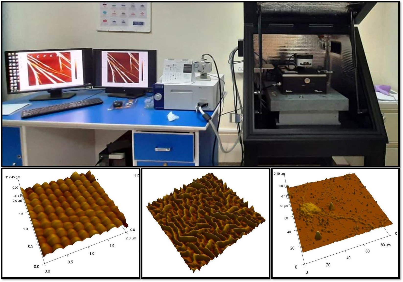
Description: "MFP-3D Origin™ features high-resolution imaging, supports large samples, most imaging modes, and many accessories. High-resolution imaging in both air and fluid — 120 µm XY range and 15 µm Z (40 µm optional) Nanomechanical characterization modes available for measuring viscoelastic properties (storage/elastic modulus and loss modulus) Large range of nanoelectrical and electromechanical characterization modes"
Literature based on this facility:
- Nanocarbon-Enforced Anisotropic MusCAMLR for Rapid Rescue of Mechanically Damaged Skeletal Muscles
- Vanadium dioxide thin films synthesized using low thermal budget atmospheric oxidation
- Ultra-Fast, Chemical-Free, Mass Production of High Quality Exfoliated Graphene
- High infrared reflectance modulation in VO2 films synthesized on glass and ITO coated glass substrates using atmospheric oxidation of vanadium
- Direct use of RAPM in laboratory study on diffusion between asphalt binders
- Exfoliating a CdII–Purine Framework: Conversion of Nanosheets-to-Nanofibers and Studies of Elastic and Capacitive Properties
- Tripeptide-induced modulation of mesenchymal stem cell biomechanics stimulates proliferation and wound healing
- To study surface and sub-surface nanomechanical properties of electrospun polyacrylonitrile (PAN) nanofibers/polydimethylsiloxane (PDMS) composites
- A cross-linked polymer inclusion membrane for enhanced gold recovery from electronic waste
- Effect of cross-linking on the performance of polymer inclusion membranes (PIMs) for the extraction, transport and separation of Zn(II)
Partical Size Analyzer
- Instrument Name: Beckman Coulter
- Make (Manufacturer): NA
- Model: Delsa Nano C
- Function: : Size and Zeta Potential measurement of particles in liquid suspension.
- Company URL: Atomic Force Microscopy (AFM)
- Operator: Ms. Deepali Ubale
- Contact: 0512 259 6385
- E-mail: ubaled@iitk.ac.in

Description: Photon correlation spectroscopy and electrophoretic light scattering ,Measurement range: Size: 0.6nm-7um, Zeta Potential: +/-100mV Sample concentration: 0.001% to40%, Minimum sample volume: Size: 60uL Zeta Potential: 2ml,Scattering Angles(s):15, 30, 165 deg.,Light Source: 2Lasers diodes, Wave Length: 658 nm, Intensity: 30mW Delsa Nano C is a photon correlation spectroscopy (PCS) instrument, which determines particle size by measuring the rate of fluctuations in laser light intensity scattered by particles as they diffuse through a fluid. For measuring the zeta potential, it determines electrophoretic movement of charged particles under an applied electric field. The Delsa Nano also can measure zeta potential (or surface charge) of a solid surface or film.
Contact Angle Measurement (Goniometer)
- Instrument Name: NA
- Make (Manufacturer): Kruss
- Model: DSA 25 (Drop Shape Anaylzer)
- Function: : NA
- Company URL: Goniometer
- Operator: Ms. Deepali Ubale
- Contact: 0512 259 6385
- E-mail: ubaled@iitk.ac.in

Description: "In its Expert configuration, the DSA25 Drop Shape Analyzer is designed for determining the wettability of solids by means of the contact angle as well as the surface tension of liquids such as coating substances or adhesives. The combination of speed and versatile evaluation options, the analyses give quick feedback to pretreatment steps in quality control but also allow assessing the resulting adhesion.Helps in measuring Static contact angle,Contact angle using a bubble in a liquid , Surface free energy (SFE) according to the following models: Owens-Wendt-Rabel-Kaelble (OWRK), Fowkes, Wu, Zisman, Equation of State, Work of adhesion, solid/liquid interfacial tension, spreading coefficient, Advancing and receding contact angle,roll-off angle,Surface tension of a liquid and interfacial tension between two liquids.
Nulling Ellipsometry and Microscopy
- Make (Manufacturer): Accurion
- Types of sample to be analyse: Thin film only
- Modes Available: Single wavelength 532nm, Spectroscopy 300nm- 1000nm, SPR
- Company URL:Ellipsometry
- Operator: Dr Seema Sharma
- Contact: 0512 259 6264
- E-mail: seemas@iitk.ac.in

- Direct sample visualization with an ellipsometry contrast image with a lateral resolution as small as 1 micron
- Imaging ellipsometry in the wavelength range from 250 nm to 1700 nm
- High range of accessories to cope with a variety of applications (SPR or solid/liquid cells, light guide for liquid/liquid interfaces, microfluidic, temperature control, electrochemistry cells and many more)
- Real time ellipsometry contrast images provide a fast view of the surface, any defects or structures
- Parallel measurement of multiple areas within the selected field of view
- Knife edge illumination avoids background reflection and allows measurements on thin transparent substrates
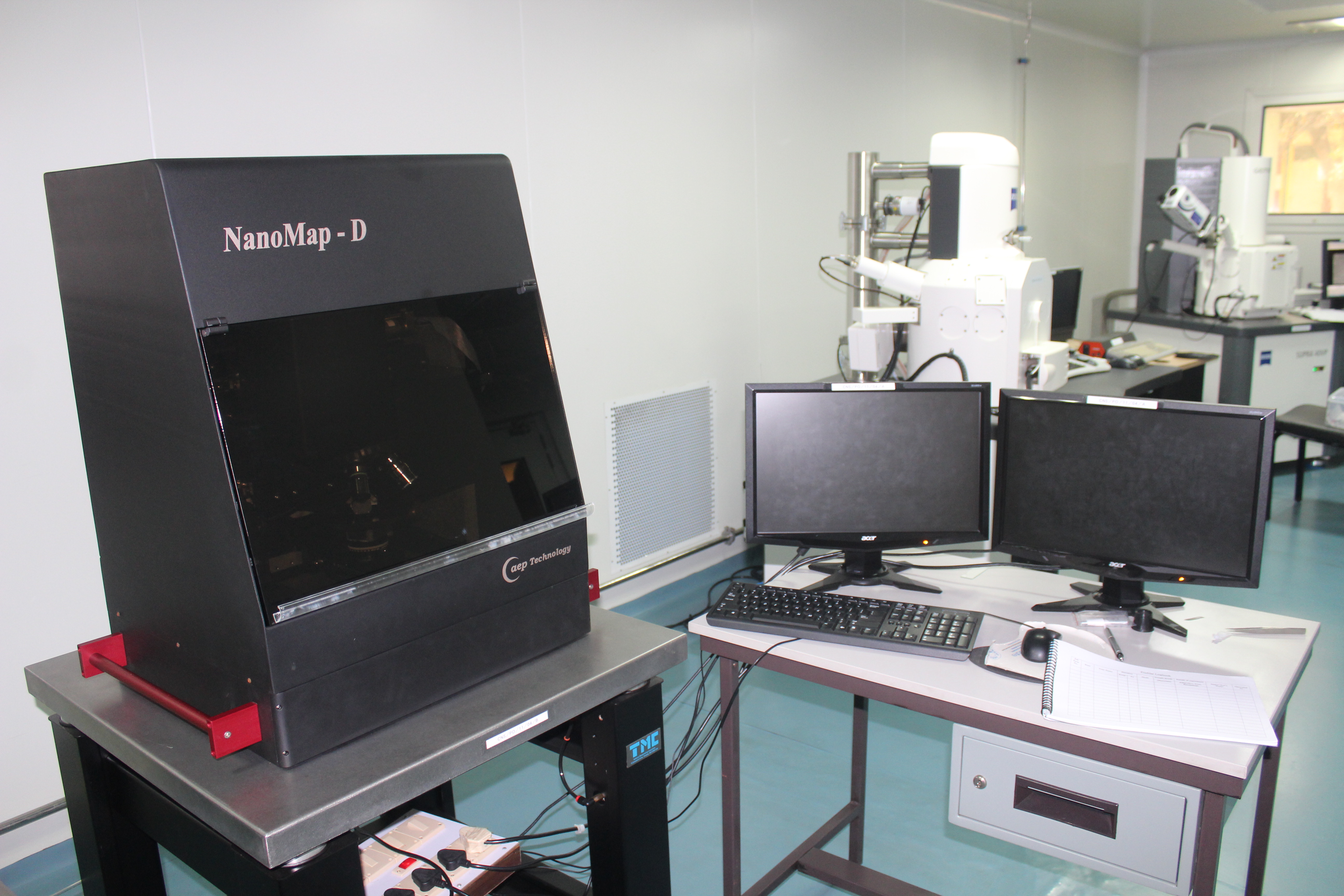
3D Profilometer
- Make (Manufacturer): Aep Technology, Nanomap D (Dual Mode)
- Types of sample to be analysed: : Thin film, Solid Sample.
- Modes Available: Optical Profilometer, Contact Profilometer.
- Company URL: Link
- Operator: Dr Seema Sharma
- Contact: 0512 259 6264
- E-mail: seemas@iitk.ac.in
- Rotation (theta)-360 Degree
- Pixel Standard-1024 x 1024, Optional 1536 x 1536 or 1920 x 1920 (optical mode)
- Optical Camera Color camera with-1.5 x 1.5mm FOV(contact mode)
- Step heights measurement
- Surface Roughness measurement
- Quantify scratch and dig features, wear depth, width and volume
- Flatness or curvature measurement
- 2D thin film stress measurement
- Film thickness
- Surface Profiling - defect, features etc
Limitation:
- Optical Mode: Vertical Resolution- 0.1nm, 0.02nm, Scan Range Up to-150mm x 150mm (Optional 200mm or more), objective – 5x, 20x, 50x. Z focusing range-0.1 nm to 10mm
- Contact Mode: Vertical Resolution-0.1nm with fine range; 0.01um with coarse range, Vertical Dynamic Range-Up to 5um with fine range; up to 2000um with coarse range, Scan Range-Up to 150mm x 150mm (upgrade available), XY Piezo Stage Resolution-0.1um, Stylus Loading Force-0.01mg to 100mg,
Fourier Transform Infrared spectrophotometer (FTIR)
- Make & Model: Spectrum 2, Perkin Elmer
- Modes Available: Transmission , ATR ( for surface analysis)
- Types of material analysed : Thin film, Powder, Solids.
- Derails link: Details
- Operator: Ms. Seema Sharma
- Contact: 0512 259 6264
- E-mail: seemas@iitk.ac.in
Description: Fourier-transform infrared spectroscopy (FTIR) is a technique used to obtain an infrared spectrum of absorption or emission of a solid, liquid or gas. An FTIR spectrometer simultaneously collects high-resolution spectral data over a wide spectral range.
UV-Vis Spectrophotometer
- Make & Model: Bio 50, Varian
- Approved Abbreviation:UV - Visible Spectrophotometer
- Make (Manufacturer): Varian UV
- Model: Cary 50 Bio
- company URL:www.varianinc.com
- Description:
- Range: 0-1200
- Modes: Absorption and Transmission
- Derails link: Click Here
- Types of material analysed : Thin film
- Types of sample analysed : Liquid
- Operator: Ms. Seema Sharma
- Contact: 0512 259 6264
- E-mail: seemas@iitk.ac.in

Description: Ultraviolet–visible spectroscopy or ultraviolet–visible spectrophotometry (UV–Vis or UV/Vis) refers to absorption spectroscopy or reflectance spectroscopy in part of the ultraviolet and the full, adjacent visible regions of the electromagnetic spectrum.
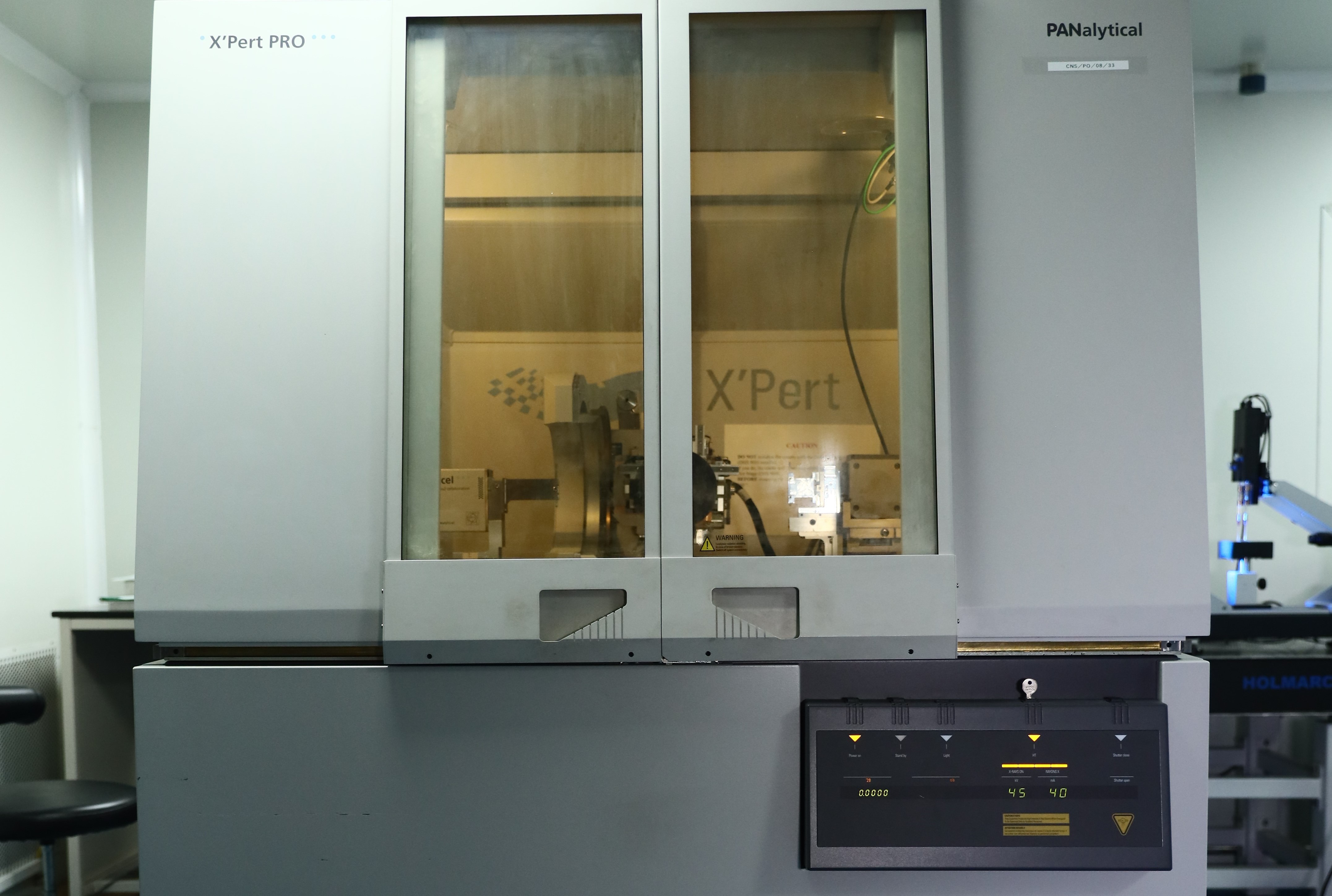
X-Ray Diffraction Machine (XRD)
- Make & Model: Multi-purpose Diffractometer, Panalytical
- Modes Available: Powder XRD, Thin Film Grazing Indices, Rocking Curve, Non ambient temperature
- Types of material analysed : Thin film, Powder, Solids.
- Derails link: Details
- Operator: Ms. Seema Sharma
- Contact: 0512 259 6264
- E-mail: seemas@iitk.ac.in
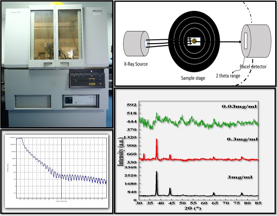
Description: X-ray diffraction is a powerful non-destructive technique for characterizing crystalline materials. It provides information on structures, phases, preferred crystal orientations (texture), and other structural parameters, such as average grain size, crystallinity, strain, and crystal defects.
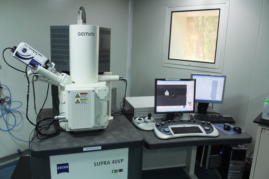
FESEM
- Approved Abbreviation: Field Emission Scanning Electron Microscope
- Make (Manufacturer): Zeiss
- Model: SUPRA 40 VP
- Company URL: www.zeiss.co.in
- Description: The Zeiss Supra 40VP scanning electron microscope provides high resolution surface imaging with three-dimensional appearance. It is equipped with a field emission cold cathode as electron source and two different detectors (SE2, InLens). It can be used for fixed, critical point dried samples as well as for fresh material in variable pressure mode or for fresh biological samples.
- Maximum resolution: 1 nm
- Magnification range: 100x - 900,000x
- Acceleration voltage: max. 30 kV
- Software: SmartSEM
- Operator: Mr. Abhishek Bajpai
- Contact: 0512 259 6264
- E-mail: abhishekb@iitk.ac.in
SEM
- Approved Abbreviation: Scanning Electron Microscope
- Make (Manufacturer): Zeiss
- Model: EVO 18
- Company URL: www.zeiss.co.in
-
Description: EVO 18 provides excellent quality imaging results from an analytical microscope with the capability to handle all material types.
At low kV, the performance and enhanced topography information is offered on EVO 18 by the 5 segment diode BSE detector. For non-conducting samples, user can increase analytical resolution by using the optional BeamSleeve (at VP mode).
The Evo18 is coupled with the ease-of-use provided by SmartSEM software, EVO 18 Research is perfectly suited to a variety of research applications including Semiconductor and Electronics, Geoscience and Materials. - Maximum resolution: 20 nm
- Magnification range: 100x - 100,000x
- Acceleration voltage: max. 30 kV
- Software: SmartSEM
- Operator: Mr. Abhishek Bajpai
- Contact: 0512 259 6264
- E-mail: abhishekb@iitk.ac.in

Fluorescence Microscope
- Make & Model: ZEISS India
- Make (Manufacturer): Varian UV
- Model: XENOX, Serial no. 3837000164
- company URL:www.zeiss.com
- Types of material analysed : Rhodamine-6G, cells
- Types of sample analysed : Chemically synthesized films, Biological samples
- Operator: Ms. Sayma
- Contact: 0512 259 6264
- E-mail: saymaa@iitk.ac.in
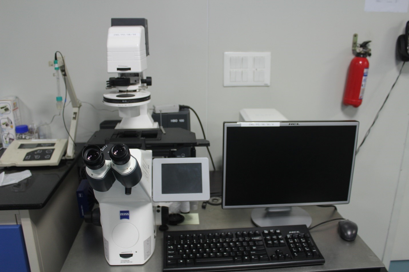
Description: Examination of fluorescently labeled cells and tissues