| |
|
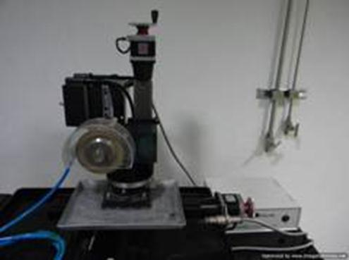
2-D PIV
|
2C-PIV is an optical technique which measures the velocity field in a plane. The flow field is seeded with tracer particles. A pulse laser with combination of cylindrical and spherical lens illuminates a plane with a laser sheet. The pulse separation is about nano-second which is adjusted depending on the magnitude of velocity measured. The laser is synchronized with a camera for acquisition of the image at same time instant. The cross correlation between two consecutive images provides the displacement of particles and the velocity. The 2C-PIV has been updated to stereo-PIV (3C-PIV) from support by Naval Research Board for measurement of all three components of velocity.
Technical Specifications:
Laser: Nd:YAG, New Wave
Laser Power: 15 mJ/pulse
Camera: PCO Sensicam 1280 X 1024 pixel
Synchroniser: Oxford Lasers
PIV Processing: Vid PIV
|
Location:
|
Fluid Mechanics Laboratory, RN: 301, Department of Mechanical Engg.
IIT Kanpur
|
Contact:
|
Prof. P. K. Panigrahi
This email address is being protected from spambots. You need JavaScript enabled to view it.
|
|
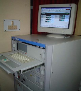
RF Analog Signal Generator Facility
|
Radio frequency signal generators (RF signal generators) are a particularly useful item of test equipment widely used in RF design and test applications. E8257D PSG analog signal generator delivers a sufficient level of output power, accuracy, and phase noise performance up to 20 GHz. The PSG analog signal generator's often eliminates the need of an external amplifier for testing high power devices and minimizes test uncertainty to identify errors early in the design process.
Unique features:
Signal Characteristics (250 kHz to 20GHz, 23dbm@20GHz), High SSB phase noise performance, Modulation (AM, FM, ØM, pulse, and scan), 8 ns rise/fall times and 20 ns pulse width, Dual internal function generators (sine, square, triangular), and Step, ramp sweep (frequency and power) etc.
|
Location:
|
Microwave Circuit Laboratory, Department of Electrical Engineering,
IIT Kanpur
|
Contact:
|
Prof. Kumar Vaibhav Srivastava
This email address is being protected from spambots. You need JavaScript enabled to view it.
|
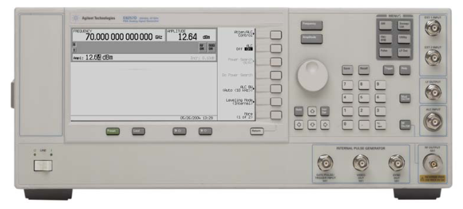 Fig: 1 Fig: 1
|
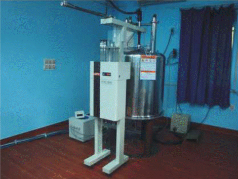
400 MHz NMR Machine with upgraded Console
|
Procures in the Financial Year: 2011-12 The machine is fully functional and is one of the most essential tools for structural characterization.
|
Location:
|
Core Lab 106b,
IIT Kanpur
|
Contact:
|
Prof. Ramesh Ramapanicker
This email address is being protected from spambots. You need JavaScript enabled to view it.
Dr. Anand Singh
This email address is being protected from spambots. You need JavaScript enabled to view it.
|
User Charges:
|
INR 10.00 per sample for 1H NMR
INR 25.00 per sample for 13C NMR
(Service tax is applicable for non-IITK users)
|
|
|
A Probe Station for Temperature and Magnetic Field Dependent Electrical measurements on thin films, devices and materials
|
Procures in the Financial Year: 2010-11
Capabilities:
Temperature dependent probe station with capabilities to make electrical measurements from 20K to 600K.
|
Location:
|
Western Lab – 105,
IIT Kanpur
|
Contact:
|
Prof. Ashish Garg
This email address is being protected from spambots. You need JavaScript enabled to view it.
|
|
User Charges:
|
Rs. 1000/- per 3 hrs slot
(Service tax is applicable for non-IITK users)
|
|
|
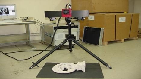
Advanced Topometric Optical Sensor (ATOS)
|
Computer-aided techniques like CAD, CAM and FEM require an efficient coordinate measuring technique in order to achieve exact correspondence between numerical model and real component. Using the digitizing system ATOS (Advanced Topometric Sensor), an object can be measured in a short time and with high local resolution. Each single measurement generates up to 1.3 million data points. The individual measurements are merged into a project and the measured data can be exported as point clouds, sections or STL-data. Additional hardware, such as mechanical measuring machines, translation units or robots, is not required.
Features:
The user can concentrate on the digitizing progress as all the transformations are performed automatically by the system.
The same sensor (ATOS XL) is capable of measuring small and large objects (10mm up to 10m).
Due to the high point density, details of the component can be depicted precisely. The accuracy of the measured data is comparable to that of single frame coordinate measuring machines.
The system can be transported in two flight cases (part of the standard equipment) by car or plane
|
Location:
|
CAD Lab, Department.of Mechanical Engineering,
IIT Kanpur
|
|
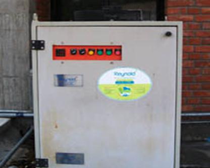
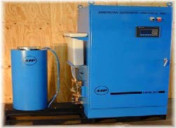
Air Cooled Chiller
|
A chiller is a machine that removes heat from a liquid via a vapor-compression or absorption refrigeration cycle. A vapor-compression water chiller comprises the 4 major components of the vapor-compression refrigeration cycle (compressor, evaporator, condenser, and some form of metering device). The chiller will be used to fed the PECVD/ Sputtering systems etc.
|
Location:
|
NET building, Department.of Mechanical Engineering
IIT Kanpur
|
Contact:
|
Prof. Shantanu Bhattacharya
This email address is being protected from spambots. You need JavaScript enabled to view it.
|
|
Artec MHT™ 3D Scanner
|
The Artec MHT scanner captures brilliant color at up to 24 bits per pixel. That means that the resulting texture is of great quality similar to a modern video camera. This model is perfect for designers, movie makers and animators. Also, this is a great tool for those in the heritage preservation industry, because capturing the enchanting coloring of a clay pot from ancient Greece is just as important as capturing its shape. This is the appropriate choice for those that need to not only acquire 3D data, but the color of the object as well.
Heritage Preservation
Artec 3D Scanners are portable, phenomenally quick and can be used with objects of various sizes. There’s no need to move scanned items or to place markers on the object. These are the advantages that make our 3D Scanners an indispensable tool in the preservation of the world’s cultural heritage.
Restoration
Restoration of interiors and entire buildings means reproducing missing features of the decor. This means obtaining exact 3D copies of features of sculpture, architecture, stucco ornaments or fragments of antique furniture. Artec 3D Scanners enable users to carry out these tasks with ease and concentrate on producing the items needed in order to restore the original look.
Archives and catalogues
The Artec 3D Scanner can be used to make copies of items found in the course of archaeological or palaeontological work, such as fragments of ceramics or bone. This means databases can be set up and made accessible to researchers.
|
Location:
|
CAD Lab, Department of Mechanical Engineering,
IIT Kanpur
|
AMBIOS Surface Profilometer
|
Ambios Profilometer is a computerized, high- sensitivity surface profiler that measures roughness and step height in a variety of applications. It features the ability to measure precision step heights from under 10 Angstroms to as large as 1.2 millimetres. The profiler incorporates a new optical deflection height measurement mechanism and magneto static force control system that results in allow force (loads as small as 0.03mg) and low inertia stylus assembly. These innovations combine to produce a surface profiler capable of measuring soft films and substrates without surface damage. Simply position your sample on the scan stage, select a scan recipe, click the scan button, and as soon as the scan is complete, your surface data is immediately available for analysis. The XP-100 Profilometer provides an affordable, high resolution surface measurement capability that nicely complements other analytical instruments.
Profilometer provides following features:
-
Scan Length range- 30mm maximum
-
Sample Thickness -20mm
-
Vertical resolution- 100nm
-
Vertical range -1200um maximum
-
Step height repeatability 5Ao
-
Repeatability: approx 1um step height
-
Sample view camera- colour camera
-
Standard magnification- 100X
-
Stylus tip radius -2.5um
-
Stylus force range -0.03-10mg
|
Location:
|
Clean Room - P2, Samtel Center for Display and Technology (SCDT),
IIT Kanpur
|
Contact:
|
Mr. Dharmendra Swain
This email address is being protected from spambots. You need JavaScript enabled to view it.
|
Atomic Absorption Spectrometer
|
The Atomic absorption (AA) spectrometer is used to analyze metals at very low concentrations, typically in the parts per million (ppm) or parts per billion (ppb) ranges. A liquid sample containing dissolved material whose concentration is to be measured is aspirated into a thin, wide AA flame, or is introduced into a small carbon furnace which is heated to a high temperature. The Atomic absorption (AA) spectrometer (Varian AA240) (Figure 1) was established in the Core Lab (201D) in 2007 with the DRDO grant of the Institute.
Basic Principle:
AAS is the measurement of absorption of radiation by free atoms. The total amount of absorption depends on the number of free atoms present and the degree to which the free atoms absorb the radiation. At the high temperature of the AA flame, which may be either oxy-acetylene as used here, or nitrous oxide/acetylene, the sample is broken down into atoms and it is the concentration of these atoms that is measured (Figure 2).
Unique Features:
Fast Sequential capabilities with four lamps, so we can determine more elements in rapid sequence from one sample analysis. Fully automatic wavelength and slit selection simplifies operation, even for novice users. Completely sealed optics with quartz overcoated mirrors offer protection in dusty or corrosive environment. The air purge system is fitted inside the instrument eliminating the chance of corrosion in rugged or corrosive environments.
|
Location:
|
Department of Chemical Engineering, Core Lab 201D,
IIT Kanpur
|
Contact:
|
Prof. Nishith Verma
This email address is being protected from spambots. You need JavaScript enabled to view it.
|
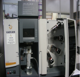
Figure 1
|
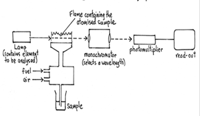
Figure 2
|
Atomic Force Microscope
|
Atomic Force Microscope and is often called the "Eye of Nanotechnology". AFM is a high- resolution imaging technique that can resolve features as small as an atomic lattice in the real space. It allows to observe and manipulate molecular and atomic level features. This AFM is capable of scanning large areas with high resolution. Conducting AFM, MFM, imaging in liquid media, atomic level manipulations, dip pen lithography and local anodic oxidation are some of the salient features of this microscope
|
Location:
|
Thematic Unit of Excellence,
IIT Kanpur
|
Contact:
|
Prof. Ashutosh Sharma
This email address is being protected from spambots. You need JavaScript enabled to view it.
Dr. Prabhat Dwivedi
This email address is being protected from spambots. You need JavaScript enabled to view it.
Dr. Dinesh Deva
This email address is being protected from spambots. You need JavaScript enabled to view it.
|
|
Atomic Force Microscopy facility (Park XE 70)
|
Users desirous of using the facility may fill up the booking form available at http://home.iitk.ac.in/~sar/AFM_CARE2013.pdf. A new Atomic Force Microscopy facility has been established under the CARE funding 2013 and is now operational. The AFM is a Park XE 70 machine with a 100micron X 100 micron scanner head and a liquid cell.
Application:
Accurate XY Scan by Crosstalk Elimination
-
Independent, loop XY and Z flexure scanners for sample and probe tip
-
Flat and orthogonal XY scan with low residual bow
-
Out of plane motion of less than 2 nm over entire scan range
-
Accurate height measurements without any need of software processing
Best Life, by True Non-ContactTM Mode
-
10 times faster Z-servo speed than competing AFM piezo tube
-
Less tip wear for prolonged high-quality and high-resolution imaging
-
Minimized sample damage or modification
-
Immune from parameter-dependent results observed in tapping imaging
The Most Extensible AFM Solution
-
The most comprehensive range of SPM modes
-
The largest number of sample measurement options
-
The best option compatibility and upgradeability in the industry
The Best User Convenience by Design
-
Open side access for easy sample or tip exchange
-
Easy, intuitive laser alignment with pre-aligned tip mount
-
Easy head removal by dovetail-lock mount
-
Direct on-axis optics for high resolution optical viewing
Features:
|
User Charges: :
|
Rs. 1000 for 2 hours A user fee of Rs.1000 for a 2 hour slot will be applicable.
|
Location:
|
Department of Physics
IIT Kanpur
|
Contact:
|
Prof. S. Anantha Ramakrishna
This email address is being protected from spambots. You need JavaScript enabled to view it.
|

|
BET Surface Area & Pore Volume Analyzer
|
Quanta chrome Autosorb 1C BET Surface Area & Pore Volume Analyzer is an instrument to determine the specific surface area of powders, solids and granules, the values are expressed in meter square per gram, pore size analysis, micropore analysis, pore size distribution by pore diameter, pore volume and pore surface area. The Quanta chrome Autosorb 1C BET Surface Area & Pore Volume Analyzer (Figure 1) was established in the Core Lab (201D) in 2009 with FIST (DST) grant of the Institute.
Basic Principle:
The adsorption/desorption isotherms and pore volumes of the adsorbents were determined by nitrogen adsorption–desorption isotherms, measured at 77 K using Quanta chrome Autosorb 1C system. The samples were degassed at 200°C under vacuum before starting N2 adsorption. Surface area and pore volumes (or pore size distribution) were determined using the Brunauer–Emmet–Teller (BET) equation, Barret–Joyner–Halenda (BJH) and DFT methods respectively.
Unique Features:
Automatically performed Temperature programmed techniques (TPR/TPD/TPO. Flow-based, pulse titration method for rapid determination of active surface area, degree of metal dispersion. Available vapor generator option with heated manifold for use with water and organic vapors. Available, integrated mass spectrometer option for identification of desorbed gases. High sensitivity, thermal conductivity detector (TCD) for TPR/TPD/TPO analysis and automatic physisorption and chemisorption by precise vacuum volumetric method for analysis of BET surface area, meso- and micropore size distribution, active surface area, degree of metal dispersion, heats of adsorption, etc.
|
Location:
|
Department of Chemical Engineering, Core Lab 201D,
IIT Kanpur
|
Contact:
|
Prof. Nishith Verma
This email address is being protected from spambots. You need JavaScript enabled to view it.
|
Figure 1
|
Figure 2
|
Brewster Angle Microscope
|
EP3-BAM is an ideal thin films imaging system. It is a completely "hands-off" computer-controlled system, using proprietary motor control circuitry. The EP3-BAM displays real-time image of your sample directly on the monitor and features important image processing functions. An "objective scanner" provides extended depth-of- field for overall-focused images. The combination of a high power green laser and excellent objectives allows lateral resolutions of 1 micron, the current limit of CCD optical detectors. The powerful software makes operation easy and convenient. As a complete solution, the system comes including the computer, electronics, and all necessary software needed to begin measurements on your existing trough, or with one of our integrated NIMA troughs
|
Location:
|
Thematic Unit of Excellence,
IIT Kanpur
|
Contact:
|
Prof. Ashutosh Sharma
This email address is being protected from spambots. You need JavaScript enabled to view it.
Dr. Prabhat Dwivedi
This email address is being protected from spambots. You need JavaScript enabled to view it.
Dr. Dinesh Deva
This email address is being protected from spambots. You need JavaScript enabled to view it.
|
|
CAMAG HPTLC System with AMD2
|
High Performance Thin Layer Chromatography is capable of separating organic compounds. Automated multiple development adds flexibility and enhance reproducibility and quantification. The user need to have knowledge of layers and solvents to be used for separation. In the absence of this knowledge, a method development step is necessary. The sensitivity of thin layer chromatography is less than gas or liquid chromatography. However, it is fast, standards and samples can be analyzed simultaneously on the same plate, versatile about the sample solvent and cheapest amongst all the chromatographic applications
Technical Specifications:
Components available are: Linomat 5 for sample application, AMD2 for automated multiple development, twin trough tanks of different sizes for manual single solvent developments, HPTLC vario system for method development, TLC Scanner 3 for detection, TLC/HPTLC documentation system with digital camera, Reprostar TLC/HPTLC viewing box with UV system, TLC plate heater, TLC plate coater, dip tanks, dedicated computer with win CATS Planar Chromatography System Manager.
|
Location:
|
Environmental Engineering Laboratory, WL 116
IIT Kanpur
|
Contact:
|
Prof. Saumyen Guha
This email address is being protected from spambots. You need JavaScript enabled to view it.
|
|
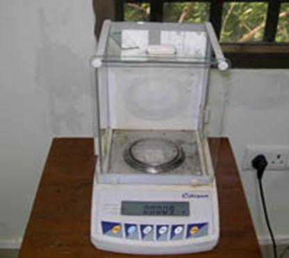
Chemical Balance
|
A beam balance of great precision used in quantitative chemical analysis.
|
Location:
|
NET building, Department.of Mechanical Engineering
IIT Kanpur
|
Contact:
|
Prof. Shantanu Bhattacharya
This email address is being protected from spambots. You need JavaScript enabled to view it.
|
|
| |
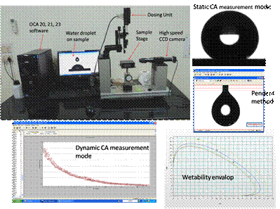
Procures in the Financial Year: 2011-12
The machine "Contact Angle Goniometer" is designed to investigate interfacial properties (surface free energy, wettability, surface/interfacial tension) of solid-solid, solid-liquid and liquid-liquid interface. The machine is designed with four software controlled dosing unit (electronic syringes) to eject controlled amount of various liquids on a solid surface. The machine has normal as well as high speed imaging capability to explore static and dynamics of interfacial properties. It also has an environmental chamber to manipulate environmental conditions e.g. temperature, humidity, gas and study its effect on interfacial properties.
|
Location:
|
Southern Lab 20,
IIT Kanpur
|
Contact:
|
Prof. Krishnacharya
This email address is being protected from spambots. You need JavaScript enabled to view it.
|
|
User Charges:
|
For a 2 hour slot:
Contact angle/surface tension measurement (ambient condition) INR. 200/-
Interfacial tension (between two fluids) measurement (ambient condition) INR. 500/-
Surface free energy of solid measurement (ambient condition) INR. 1000/-
Measurement involving environmental chamber (variable temp, humidity) INR. 2000/-
Measurement involving high speed camera (upto 1000 fps) INR. 2000/-
(Service tax is applicable for non-IITK users)
|
|
|
Contact Angle Tensiometer Facility
|
Model OCA EC15 from Data Physics, GmbH, Germany
Surface properties such as wetting behavior, surface free energy and its polar and dispersion components significantly affect the end use of the material in numerous ways. Some of the examples are hydrophobicity ND hydrophilicity of implanted material that affect cell adhesion, surface energy that affects spreading of liquid ink in printable electronics, adsorption behavior of packaging material in food packaging industry, etc. Therefore, it is necessary to evaluate the surface properties of engineering material.
Specifications:
Dosing volume up to 0.1μl; Temperature variation (5-90°C); Advancing and receding contact angle measurement (-20 to 70°); OCA 23 software equipped with surface energy calculation; Large database of scientific liquids; adsorption rate of liquid on specimen; contact angle between two immiscible liquids.
|
Location:
|
Biomaterials Processing & Characterization Laboratory (behind Western Laboratories)
IIT Kanpur
|
Contact:
|
Prof. Kantesh Balani,
This email address is being protected from spambots. You need JavaScript enabled to view it.
,
|
|
Control Systems Laboratory
|
Facilities:
18 benches, each with
- A permanent magnet dc motor control setup built around a dsPIC30F4012 microcontroller
- Function generator
- Power supply
- PC with MPLAB IDE, GNU Octave, etc.
Each setup is capable of communication with the remaining setups using Controller Area Network (CAN) protocol. This experimental setup was developed in the NCS Laboratory.
|
Location:
|
Department of Electrical Engineering
IIT Kanpur
|
Contact:
|
Prof. Ramprasad Potluri
This email address is being protected from spambots. You need JavaScript enabled to view it.
|
CARL ZEISS AXIO IMAGER A1m RESEARCH TRINOCULAR REFLECTED LIGHT MICROSCOPE FOR BRIGHT FIELD, CIRCULAR DIC.
|
The AxioImager A1m microscope features the EC Epiplan-Neofluar Lens, which supplies substantially more visible information, and the Differential Interference Contrast in Circular polarized light (C-DIC) contrasting technique that makes all image information visible without stage rotation, in addition to providing greater contrast and image clarity. (NO TRANSMISSION IMAGE FACILITY & CAMERA ATTACHMENT
Minimization of stray light components that reduce contrast are created by residual reflections of the lens surfaces and reflections at the edge of the mount. Via specific target functions in the optics correction procedure that influence the rest of the optical imaging procedure for lens surface reflections, and through careful selection of antireflection coatings, the residual light components created by single and multiple reflections on the lens surfaces are manipulated so that they can no longer have a significant effect on the contrast in the image plane.
Special features:
Axio Imager. A1m microscope stand incl. Z-drive man., reflected-light illumination with aperture stop and luminous-field diaphragm, with DIC Objectives: Epiplan5x/0.13DIC M27(a=15.8mm), 10x/0.25DIC M27(a=9.3mm), 20x/0.22 M27 (a=12.1mm), 50x/0.55 DIC M27 (a=9.1mm), 100X on Order, and Eyepiece 10x/23 Br. Foc
|
Location:
|
Optoelectronics Laboratory, Department of Electrical Engineering,
IIT Kanpur
|
Contact:
|
Prof. Utpal Das
This email address is being protected from spambots. You need JavaScript enabled to view it.
|
|
Cary 5000 UV-Vis-NIR Spectrophotometer
|
The Cary 5000 can be used to achieve significant performance breakthroughs across a range of applications; from simple optical absorbance and reflectance measurements in the wavelength range (175-3300 nm) for solid and liquid samples to quantifying out-of-band blocking characteristics of band pass filters and also measuring the high transmission of next generation fibre optic materials.
Salient Features:
Wavelength Range 175-3300 nmOptical Isolation System Solid aluminium casting that isolates the optics from external disturbances. i.e. laboratory environment won't affect your instrument's performance. Pb smart technology where PbS NIR detector provides best noise and linearity performance Schwarzchild Coupling Optics: Ensures the maximum level of light throughput resulting more accurate measurements at low transmission levels Variable and Fixed slits: Allows optimum control over data resolution. The spectral bandwidth can be set down to 0.01 nm. The slits can be fixed in the NIR as well as the UV-Vis regions Out-of-plane double Littrow monochromator Minimizes photometric noise and stray light, providing excellent resolution Advanced electronics design: The instruments can typically measure beyond 8 Abs with reference beam attenuation Nitrogen purging: Monochromator and sample compartments have separate nitrogen purging capabilities, allowing the sample compartment to be purged at a higher rate than the instrument. Praying Mantis Diffuse Reflection Accessory (DRA) Praying Mantis is the diffuse reflectance accessory that is used for easy and reliable diffuse reflection analysis of solids and powders. It incorporates two 6:1, 90° off-axis ellipsoids which form a highly efficient diffuse reflection illumination and collection system. This unique configuration deflects the specular reflectance away from the collecting ellipsoid, minimizing the associated spectral distortions. The Praying Mantis also can be configured to study materials and reactions in controlled environments with the appropriate diffuse reflectance reaction chamber.
|
Location:
|
Department of Chemical Engineering, CL 201B
IIT Kanpur
|
Contact:
|
Prof. Goutam Deo
This email address is being protected from spambots. You need JavaScript enabled to view it.
|
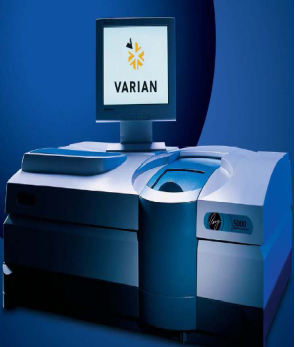
Figure: 1
|
Figure: 2
|
Figure: 3
|
Cary 5000 UV-Vis-NIR Spectrophotometer
|
The Cary 5000 can be used to achieve significant performance breakthroughs across a range of applications; from simple optical absorbance and reflectance measurements in the wavelength range (175-3300 nm) for solid and liquid samples to quantifying out-of-band blocking characteristics of band pass filters and also measuring the high transmission of next generation fibre optic materials.
Salient Features:
Wavelength Range 175-3300 nmOptical Isolation System Solid aluminium casting that isolates the optics from external disturbances. i.e. laboratory environment won't affect your instrument's performance. Pb smart technology where PbS NIR detector provides best noise and linearity performance Schwarzchild Coupling Optics: Ensures the maximum level of light throughput resulting more accurate measurements at low transmission levels Variable and Fixed slits: Allows optimum control over data resolution. The spectral bandwidth can be set down to 0.01 nm. The slits can be fixed in the NIR as well as the UV-Vis regions Out-of-plane double Littrow monochromator Minimizes photometric noise and stray light, providing excellent resolution Advanced electronics design: The instruments can typically measure beyond 8 Abs with reference beam attenuation Nitrogen purging: Monochromator and sample compartments have separate nitrogen purging capabilities, allowing the sample compartment to be purged at a higher rate than the instrument. Praying Mantis Diffuse Reflection Accessory (DRA) Praying Mantis is the diffuse reflectance accessory that is used for easy and reliable diffuse reflection analysis of solids and powders. It incorporates two 6:1, 90° off-axis ellipsoids which form a highly efficient diffuse reflection illumination and collection system. This unique configuration deflects the specular reflectance away from the collecting ellipsoid, minimizing the associated spectral distortions. The Praying Mantis also can be configured to study materials and reactions in controlled environments with the appropriate diffuse reflectance reaction chamber.
|
Location:
|
Department of Chemical Engineering, CL 201B
IIT Kanpur
|
Contact:
|
Prof. Goutam Deo
This email address is being protected from spambots. You need JavaScript enabled to view it.
|
Figure: 1
|
Figure: 2
|
Figure: 4
|
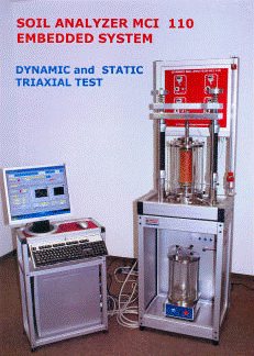
Cyclic Triaxial Testing System to Evaluate Shear Strength and Liquefaction Potential of Noncohesive Soils
|
The triaxial cyclic loading frame is designed as a stand unit in which the mechanics, pneumatic as well as the necessary electronic interface to the computer have been installed. Cyclic triaxial test is capable of applying a uniform sine, square and triangular load at a frequency within the range of 0.001 Hz to 100 Hz. The cyclic triaxial test consists of imposing either a cyclic axial deviator stress of fixed magnitude (load control) or cyclic axial deformation (stroke control) on a cylindrical soil specimen enclosed in a triaxial pressure cell. The result of axial strain and axial stress are measured and used to calculate either stress dependent or stroke-dependent modulus or damping. The cyclic triaxial modulus or damping test provides parameter that may be considered for use in dynamic, linear and non linear analytical methods. One of the primary purposes of these test method is to obtain data that are used to calculate Young’s modulus and Liquefaction Potential.
|
Location:
|
Department of Civil Engineering,
IIT Kanpur
|
Contact:
|
Prof. Nihar Ranjan Patra
This email address is being protected from spambots. You need JavaScript enabled to view it.
|
|
Data Mining Laboratory
|
Features:
Hardware:
-
High-end computers
-
High-end Color Printers
-
Video Camera
MATLAB
MATLAB (MATRIX LABORATORY) the high-performance language for technical computing. We have the compilers, plus toolboxes for image processing, optimization, signal processing, simulink, state flow, wavelets, and control.
|
Location:
|
Department of Electrical Engineering
IIT Kanpur
|
Contact:
|
Prof. Nishchal K. Verma
This email address is being protected from spambots. You need JavaScript enabled to view it.
|
Deep Reactive Ion Etch (DRIE) System
|
The Deep Reactive Ion Etching (DRIE) system was procured in 2009 with financial support from IIT Kanpur. This enables making structures in silicon, and is housed in the Centre for Environment Sciences and Engineering.
Unique Features:
An inductively coupled plasma (Figure 1) results in generation of ions and radicals which play a role in etching silicon and maintaining the required profile. The process feed gases include SF and Fluorine 6radicals and ions from SF react with the silicon surface to form volatile SiFx species and are responsible for etching. 6As the isotropic nature of the fluorine radicals would result in an isotropic etch profile, the polymerizability of CF is 48used. The radicals generated from CF deposit on the silicon surface and while the sidewalls are protected from 48lateral etch, the subsequent directional F ions remove these from the etch front for subsequent etch propagation. In the system, SF and CF are pulsed alternately into the reaction chamber which enables anisotropic etched profiles.
|
Location:
|
Center for Environmental Science and Engineering,
IIT Kanpur
|
Contact:
|
Prof. Siddhartha Panda
This email address is being protected from spambots. You need JavaScript enabled to view it.
|
Desk Top Mask Aligner
|
Mask aligners are used in most microfabrication research laboratories and in even in low- volume production facilities. Almost any microscale device or structure requires more than one photomask step. The job of the contact aligner is to allow its user to align features on a substrate (wafer) to features on a photomask. The production of sophisticated electronic devices may involve ten or more of these alignment steps.
|
Location:
|
NET building, Department.of Mechanical Engineering
IIT Kanpur
|
Contact:
|
Prof. Shantanu Bhattacharya
This email address is being protected from spambots. You need JavaScript enabled to view it.
|
|
De-ionized Water Plant with Water testing equipment
|
(a) The De-ionized water Plant comprises of two Units, the CA-20 and the MB-25. Tap water first passes through the CA-20 plant which lowers the ppm value to 10ppm. This water then passes through the MB-25 plant, which makes the water de-ionized with 0 ppm and conductivity 0 μS/cm . The meters measure in steps of 0, 10, 20, …1990 ppm or μS/cm.
(b) Water Testing equipment
- Oakton Instruments water-proof TDS tester. It can detect impurity of water from 0
to 1990 ppm, with a resolution of 10ppm. It has an automatic temperature compensation function.
- Oakton Instruments water-proof conductivity tester. It can detect conductivity from 0 to 1990 μS/cm, with a resolution of 10 μS/cm.
- pH value testing of the de-ionized water using Litmus paper.
- Testing of impurities in the de-ionized water using Chemical Setup, comprising of Silver nitrate and Nitric Acid.
This is an in-house facility and cannot be borrowed out of the Lab.
Use On Payment basis - for details see Forms in http://www.iitk.ac.in/ibc/
|
Location:
|
Ion Beam Complex, NL-105, Department of Physics, IIT Kanpur.
|
Contact:
|
Co-ordinator, IBCOR
Mr. S. Krishnasamy
Technical Superintendent, IBC
(
This email address is being protected from spambots. You need JavaScript enabled to view it.
).
Phone: 7986 / 6993
|
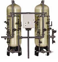
Figure: 1
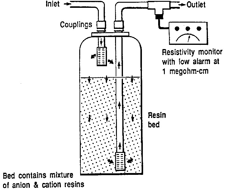
Figure: 2
|
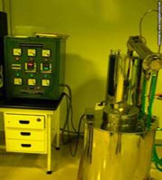
DI Water System
|
Distilled water is perfect for applications where minerals and contaminants would cause problems. Distilled water can be used in irons for steam settings or as coolant for car engines. Because there are no minerals that can stain or build up, distilled water is mostly recommended for use in machinery and cleaning products. The system produces Distiller water by heating and vaporization followed by collection and condensation of the vapours.
|
Location:
|
NET building, Department.of Mechanical Engineering
IIT Kanpur
|
Contact:
|
Prof. Shantanu Bhattacharya
This email address is being protected from spambots. You need JavaScript enabled to view it.
|
|
Dicing Saw
|
A dicing saw employs a high-speed spindle fitted with an extremely thin diamond blade to dice or groove semiconductor wafers and other work-pieces.
|
Location:
|
NET building, Department.of Mechanical Engineering
IIT Kanpur
|
Contact:
|
Prof. Shantanu Bhattacharya
This email address is being protected from spambots. You need JavaScript enabled to view it.
|
|
Digital Signal Processing Laboratory
|
Facilities:
The software facilities include the following:
-
Code Composer Studio
-
MatLab
-
LabVIEW
Test and measuring instruments:
Computers include various software and applications
-
Intel Quad Core Desktop Computer
-
Intel Pentium IV Desktop Computer
-
Intel Core I7 Desktop Computer
|
Location:
|
Department of Electrical Engineering
IIT Kanpur
|
Contact:
|
Prof. Adrish Banerjee
This email address is being protected from spambots. You need JavaScript enabled to view it.
|
Dynamic High-Resolution Polarized Inverted Laser Confocal Fluroscence Microscopy
|
Procures in the Financial Year: 2010-11
-
Inverted Microscope
-
Confocal and reflected mode operation
-
Individually controllable continuous wave lasers
-
Ar, 65mW: 458, 476, 488, 514 nm;
-
HeNe, 20 mW: 543: Green
-
HeNe, 2 mW: 633: Red
-
Multi-dimensional image capture in Space (X,Y,Z) and time (t)
-
Conventional scanning at 5 FPS at 512 X 512 pixels to 54 fps at 512 x 16 pixels
-
Typical resolution in X, Y : 200 nanometers
-
Maximum depth of view Z (depends on the objective): about 1000 microns
-
Three channel Spectrometer detector for high quality spectral image series
-
Polarizer-Analyzer Attachment
|
Location:
|
Micro-fabrication Laboratory, NL-1, Department of Mechanical Engineering,
IIT Kanpur
|
Contact:
|
Prof. P. K. Panigrahi
This email address is being protected from spambots. You need JavaScript enabled to view it.
|
User Charges:
|
Free
Note: A slot has to be booked for using the machine
|
|
|
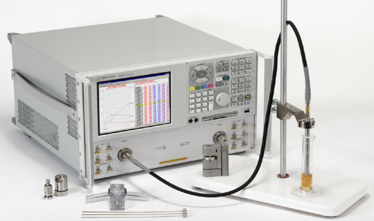
Dielectric Measurement Facility
|
The material characterization facility in the microwave frequency band was established in the Department of Electrical Engineering in the year 2010 with CARE grants from IIT Kanpur. The facility is based on the Agilent Technologies 85070E Dielectric Probe Kit, which comes along with the vector network analyzer and associated microwave components. The established facility enables one to determine the dielectric properties or the complex permittivity of wide range of materials in the broad frequency range of 200 MHz to 20 GHz. As the dielectric properties of materials are related with their molecular structure, the measurement of dielectric properties leads to much other useful information which is otherwise quite difficult to obtain. This facility (Fig. 1) is currently installed in the Microwave Imaging and Material Testing Laboratory of the department. The facility is expected to be used by departments of Civil Engineering, Bio Engineering, Material Science and Engineering, apart from the host department.
Unique features:
The dielectric probe kit is one of the most useful methods for electromagnetic characterization of materials in the broad frequency range. The complete system is based on a network analyzer, which measures the material’s response to RF or microwave energy. The probe transmits a signal into the material under test (MUT), and the reflected data is used to determine the dielectric properties of the MUT using a special software, which is supplied along with the kit. The software controls the network analyzer and guides the user through easy setup and measurement procedures. The complex permittivity of the test sample is finally displayed on screen using the supplied software.
|
Location:
|
Microwave Imaging and Material Testing Laboratory, Department of Electrical Engineering,
IIT Kanpur
|
Contact:
|
Prof. M. Jaleel Akhtar
This email address is being protected from spambots. You need JavaScript enabled to view it.
|
|
Dielectric probe kit for determination of electromagnetic properties over a wide band of frequencies
|
The dielectric measurement facility in the microwave frequency band was established in the Department of Electrical Engineering in the year 2010 with CARE grants from IIT Kanpur. The facility is based on the Agilent Technologies 85070E Dielectric Probe Kit, which comes along with the vector network analyzer and associated microwave components. The established facility enables one to determine the intrinsic electromagnetic properties of wide range of materials in the broad frequency range of 200 MHz to 20 GHz. As the dielectric properties of materials are related with their molecular structure, the measurement of dielectric properties leads to much other useful information which is otherwise quite difficult to obtain. These properties are usually expressed in terms of permittivity and permeability, which might change with frequency, temperature, orientation, mixture, pressure etc. The electromagnetic characterization facility using the dielectric probe kit is currently installed in the Microwave Imaging and Material Testing Laboratory of the Electrical Engineering department as shown in Fig. 1. The facility is expected to be used by departments of Civil Engineering, Bio Engineering, Material Science and Engineering, apart from the host department. The dielectric probe kit is one of the most useful methods for electromagnetic characterization of materials in the broad frequency range. The complete system is based on a network analyzer, which measures the material’s response to RF or microwave energy. The probe transmits a signal into the material under test (MUT), and the reflected data is used to determine the dielectric properties of the MUT using special software, which is supplied along with the kit.
|
Location:
|
Department of Electrical Engineering,
IIT Kanpur
|
Contact:
|
Prof. M. Jaleel Akhtar
This email address is being protected from spambots. You need JavaScript enabled to view it.
|
Differential Scanning Calorimetry/Thermogravitometry/Differential Thermal Analyzer (STA8000)
|
-
Compositional analysis – quantitative content analysis
-
Melting/crystallization behavior
-
Decomposition temperatures
-
Glass transition temperatures
-
Engine oil volatility measurements (TGA Noack test)
-
Specific heat capacity
-
Filler content
-
Kinetic studies
-
Flammability studies
-
Transition and reaction enthalpies
-
Lifetime predictions (via TGA kinetics software)
-
Measurement of volatiles (e.g., water, oil)
-
Oxidative stabilities
-
Thermal stabilities
-
Catalyst and coking studies
-
Hyphenation to identify out-gassing products range:
Temperature:
15 °C to 1000 °C
Balance resolution:
0.1 ug
Balance measurement range:
Up to 1500 mg
Heating rate:
Ambient to 1000°C and Cooling rates: from 1000 °C to 30 °C Under
|
Location:
|
WL210, Department of Materials Science & Engineering,
IIT Kanpur
|
Contact:
|
Prof. Krishanu Biswas
kbiswas@ iitk.ac.in
|
|
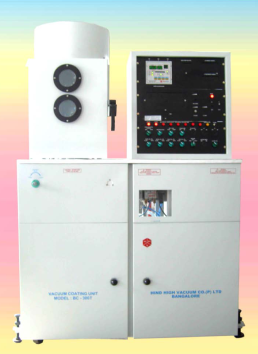
E-beam Vacuum Coating Unit – Currently Being Installed
|
Turbo pump + Mechanical Pump to 10-7 torr, 6kW e-beam, 4 –Turret with indexer.
Special features:
Digital Thickness Monitor, Turret indexer, Programmable Sweep
|
Location:
|
Optoelectronics Laboratory, Department of Electrical Engineering,
IIT Kanpur
|
Contact:
|
Prof. Utpal Das
This email address is being protected from spambots. You need JavaScript enabled to view it.
|
|
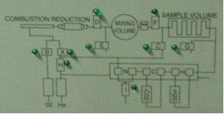
Elemental Analyzer
|
Elemental analysis is an experiment that determines the amount (typically a weight percent) of an element in a compound. A CHN/O Analyzer is a scientific instrument which can determine the elemental composition of a sample. The name derives from the three primary elements measured by the device: carbon (C), hydrogen (H) and nitrogen (N) and oxygen (O). Sulfur (S) can also be measured. The Elemental Analyzer (Exeter Analytical Inc. model: CE 440) (Figure 1) was established in the Core Lab (201D) in 2007 with the DRDO grant of the Institute.
Basic Principle:
The capsule is injected into a high temperature (1000°C) furnace and combusted in pure oxygen under static conditions. At the end of the combustion period, a dynamic burst of oxygen is added to ensure total combustion of all inorganic and organic substances. The resulting combustion products pass through specialized reagents to produce carbon dioxide (CO2), water (H2O) and Nitrogen (N2) and oxides of nitrogen. These reagents also remove other interferences including halogens, sulfur and phosphorus. The gases are then passed over copper to scrub excess oxygen and reduce oxides of nitrogen to elemental nitrogen. After scrubbing, the gases enter a mixing volume chamber to ensure a homogeneous mixture at constant temperature and pressure. The mixture then passes through a series of high-precision thermal conductivity detectors, each containing a pair of thermal conductivity cells. Between the first two cells is a water trap. The differential signal between the cells is proportional to the water concentration, which is a function of the amount of hydrogen in the original sample. Between the next two cells is a carbon dioxide trap for measuring carbon. Finally, nitrogen is measured against a helium reference (Figure 2).
Unique Features:
With unique combination of both static and dynamic combustion, the CHN/O/S instrument can combust the widest range of sample type, from volatiles to refractories. Fully automated. Rapid analysis for high productivity - analysis time of less than 5 minutes per sample. Stable thermal conductivity detector provides linear response with superior precision and accuracy. Horizontal sample injection removes interfering residue between each sample run.
|
Location:
|
Department of Chemical Engineering, Core Lab 201D,
IIT Kanpur
|
Contact:
|
Prof. Nishith Verma
This email address is being protected from spambots. You need JavaScript enabled to view it.
|
Figure 1
|
|
Encapsulation System for Organic Photovoltaic Devices/Panels
|
Organic semiconductors are recognized as emerging materials for variety of electronic devices and displays. These have the potential of making large area photovoltaic panel on large glass sheets, metal foils and polythene sheets. This will lead to cost effective manufacturing of solar modules and panels in comparison to existing technologies. To make this happen, besides increasing the efficiency of basic devices; lifetime, durability and reliability are important aspects of this technology. Organic materials in general are much more sensitive to oxygen and moisture. The problem extenuates when current is passing through it. To overcome this problem and to test different materials for their application and ruggedness for photovoltaic applications, it is imperative that the devices and panels are encapsulated under <1ppm level of oxygen and moisture levels. To meet this end, an encapsulation system has been conceptualized, designed and installed in Semiconductor Device Lab, EE Department, IIT Kanpur. It maintains oxygen and moisture levels <0.1 ppm levels. It consists of two Glove Boxes consisting of (i) a Vacuum Oven to drive out the embedded moisture and oxygen in glass plate/foils/polythene sheets, (ii) UV ozone cleaner to clean the surface, (iii) a semiautomatic UV epoxy dispenser, (iv) platform to integrate the device/panels to covering glass plate and then (v) a UV lamp to cure the epoxy. The system has been integrated to another Evaporation cum Sputtering system for fabricating the organic devices and then ransferring the same under <0.1ppm level to Encapsulation system. It is ready for use. A photograph of the system is given below.
|
Location:
|
Department of Electrical Engineering,
IIT Kanpur
|
Contact:
|
Prof. S. Sundar Kumar Iyer
This email address is being protected from spambots. You need JavaScript enabled to view it.
|
|
Establishment of a CD‐Spectrometer Facility
|
Circular dichroism is the difference in the absorption of left-handed circularly polarized light (L-CPL) and right-handed circularly polarized light (R-CPL) and occurs when a molecule contains one or more chiral chromophores (light-absorbing groups). A circular dichroism signal can be positive or negative, depending on whether L-CPL is absorbed to a greater extent than R-CPL (CD signal positive) or to a lesser extent (CD signal negative). Circular dichroism = ΔA (λ) = A (λ) LCPL - A (λ) RCPL, where λ is the wavelength. Circular dichroism (CD) spectroscopy is a spectroscopic technique where the CD of molecules is measured in the visible and ultra-violet region of the electro-magnetic spectrum. CD spectroscopy is used extensively to study chiral molecules of all types and sizes, but it is in the study of large biological molecules where it finds its most important applications. A primary use is in analyzing the secondary structure or conformation of macromolecules, particularly proteins, and because secondary structure is sensitive to its environment, e.g. temperature or pH, circular dichroism can be used to observe how secondary structure changes with environmental conditions or on interaction with other molecules. Structural, kinetic and thermodynamic information about macromolecules can be derived from circular dichroism spectroscopy. This instrument has the following features:
CD spectra measurement with wavelength
Time course CD signal measurement
Facility of variable temperature(-10ºC to 110ºC) by PTC-423S/15 Peltier effect
Quartz cells with path length 10mm, 5mm, 2mm, 1mm, 0.2mm, 0.1mm
Measurement wavelength range 163 nm to 900nm.
Stray Light less than 0.0003 % (200nm).
Wavelength repeatability ±0.05nm (163 to 250 nm) and ±0.1nm (250 to 500nm), and ±0.2nm (500 to 900nm).
|
Location:
|
Core lab no. CL107E, Department of Chemistry
IIT Kanpur
|
Contact:
|
Prof. S. P. Rath
This email address is being protected from spambots. You need JavaScript enabled to view it.
|
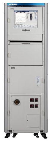
Exhaust Emission measurement system for Internal Combustion Engines
|
The proposed emission analysis system is for measurement for (UBHC) Unburnt Hydrocarbons and (NOx) Nitrogen Oxides in engine exhaust. The “RAW Exhaust EMISSION SYSTEM” is manufactured by Horiba, Japan. The EXSA 1500 emission analysis system is a modular, innovative exhaust gas emissions analysis device that can be easily adapted to user specific requirements and can be integrated into existing test environment. The EXSA complies with latest regulatory standards for light and heavy duty test procedures such as EURO III and IV. The system is designed to fulfill the research and legislative requirements for measuring gaseous emissions. The following measurement methods are applied to the regulated emission species listed
below.
|
Emission Species
|
Method
|
|
CO
|
NDIR (Non-Dispersive Infra-Red)
|
|
CO2
|
NDIR (Non-Dispersive Infra-Red)
|
|
O2
|
PMD
|
|
NOx
|
CLD (Chemiluminescence)
|
|
THC
|
FID (Flame-Ionisation Detector)
|
|
Location:
|
Engine Research Laboratory, Department of Mechanical Engneering,
IIT Kanpur
|
Contact:
|
Prof. A. K. Agarwal
This email address is being protected from spambots. You need JavaScript enabled to view it.
|
|
Faro Arm
|
The Faro Arm is a counter-balanced, temperature compensated, six degree of freedom measurement arm, constructed of anodized, aircraft aluminum with precision bearings. Proprietary, hybrid analog/digital transducers at each of six joints combine to provide complete point position (XYZ) and orientation (IJK)and makes measuring complex objects easy. This includes alignment, calibration, inspection, reverse engineering and as-built documentation.
FARO Software:
-
Surfacer (Imageware)
-
AnthroCAM
|
Location:
|
CAD Lab, Department.of Mechanical Engineering,
IIT Kanpur
|
|
FTIR based Emission Measurement System for Air Pollutant Measurement
|
Procures in the Financial Year: 2011-12
FTIR Motor Exhaust Gas Analyzer MEXA-6000FT, an engine exhaust analyzer machine is capable of measuring 36 different regulated and unregulated engine emissions. Horiba MEXA-6000FT-E is an instrument for continuously measuring the concentration of the components included in engine emissions. A combination of the Fourier Transform Infra-Red spectroscopy (FTIR) and multivariate analysis enables the simultaneous concentration analysis of multiple components. This system can be used for different fuels as diesel, gasoline, Biodiesel, CNG, LPG and other alternative fuels.
|
Location:
|
Engine Research Lab, Central Workshop Complex
IIT Kanpur
|
Contact:
|
Prof. A. K. Agarwal
This email address is being protected from spambots. You need JavaScript enabled to view it.
|
User Charges:
|
INR 2000 per sample
(Service tax is applicable for non-IITK users)
|
|
|
Fume Hood
|
A fume hood or fume cupboard is a type of local ventilation device that is designed to limit the user's exposure to hazardous or noxious fumes, vapors or dusts. A fume hood is typically a large piece of equipment enclosing five sides of a work area, the bottom of which is most commonly located at a standing work height.
|
Location:
|
NET building, Department.of Mechanical Engineering
IIT Kanpur
|
Contact:
|
Prof. Shantanu Bhattacharya
This email address is being protected from spambots. You need JavaScript enabled to view it.
|
|
Fused Deposition Modeling (FDM)
|
Fused deposition modeling (FDM) is a additive manufacturing technology commonly used for modeling, prototyping, and production applications.
The Technology:
The Fused Deposition Modelling (FDM) process constructs three-dimensional objects directly from 3D CAD data. A temperature-controlled head extrudes thermoplastic material layer by layer.
The FDM process starts with importing an STL file of a model into a pre-processing software. This model is oriented and mathematically sliced into horizontal layers varying from +/- 0.127 - 0.254 mm thickness. A support structure is created where needed, based on the part's position and geometry. After reviewing the path data and generating the toolpaths, the data is downloaded to the FDM machine.
The system operates in X, Y and Z axes, drawing the model one layer at a time. This process is similar to how a hot glue gun extrudes melted beads of glue. The temperature-controlled extrusion head is fed with thermoplastic modelling material that is heated to a semi-liquid state. The head extrudes and directs the material with precision in ultrathin layers onto a fixtureless base. The result of the solidified material laminating to the preceding layer is a plastic 3D model built up one strand at a time.
Once the part is completed the support columns are removed and the surface is finished.
Process:
FDM begins with a software process, developed by Stratasys, which processes an STL file (stereolithography file format) in minutes, mathematically slicing and orienting the model for the build process. If required, support structures are automatically generated. The machine dispenses two materials – one for the model and one for a disposable support structure.
The thermoplastics are liquefied and deposited by an extrusion head, which follows a tool-path defined by the CAD file. The materials are deposited in layers as fine as 0.04 mm (0.0016") thick, and the part is built from the bottom up – one layer at a time. FDM works on an "additive" principle by laying down material in layers. A plastic filament or metal wire is unwound from a coil and supplies material to an extrusion nozzle which can turn the flow on and off. The nozzle is heated to melt the material and can be moved in both horizontal and vertical directions by a numerically controlled mechanism, directly controlled by a computer-aided manufacturing (CAM) software package. The model or part is produced by extruding small beads of thermoplastic material to form layers as the material hardens immediately after extrusion from the nozzle. Stepper motors orservo motor are typically employed to move the extrusion head.
Several materials are available with different trade-offs between strength and temperature properties. As well as acrylonitrile butadiene styrene (ABS) polymer, polycarbonates, polycaprolactone, polyphenylsulfones and waxes. A "water-soluble" material can be used for making temporary supports while manufacturing is in progress, this soluble support material is quickly dissolved with specialized mechanical agitation equipment utilizing a precisely heated sodium hydroxide solution.
The term fused deposition modeling>and its abbreviation to FDM are trademarked by Stratasys Inc. The exactly equivalent term, fused filament fabrication (FFF), was coined by the members of the Rep Rap project to give a phrase that would be legally unconstrained in its use. It is a new model.
|
Location:
|
CAD Lab, Department.of Mechanical Engineering,
IIT Kanpur
|
|
|
|
|
|
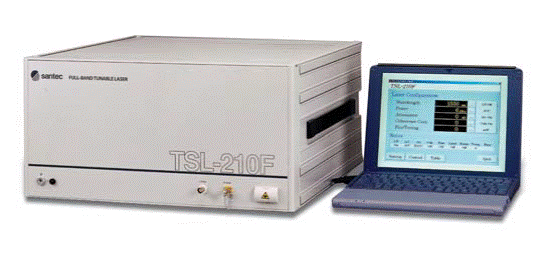
Full-Band Tunable Laser TSL-210F
|
TSL-210F is a tunable laser that covers from O band to U band. Integrating optical laser units, the TSL-210F outputs power from 1260 to 1630 nm (370nm range). It can be easily controlled via GPIB with PC and software. It has excellent cost performance and shows advantages for various research and development.
Features:
370nm wide tuning range 1260 to 1630nm
Peak >10mW, 370nm>4mW (Typ.) high output power
Easy and automatic operation by exclusive software
High accuracy and stability
Built-in OTF and OVA option available
|
Location:
|
Department of Electrical Engineering,
IIT Kanpur
|
Contact:
|
Prof. Utpal Das
This email address is being protected from spambots. You need JavaScript enabled to view it.
|
|
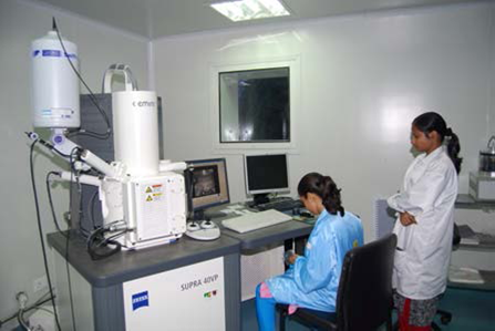
Field Emission Scanning Electron Microscope
|
The unique variable pressure capabilities add an extra dimension to this FESEM. It enables ultra high resolution imaging and analysis of non conducting specimens without time consuming preparation. The true workhorse in the SUPRA™ family is well suited for failure analysis, life sciences, nanotech and analytical applications. The combination of the large analytical chamber, the new GEMINI® column and the robust VP technology delivers true performance for a wide range of applications. It features magnification power of more than one million times.
Its resolution is up to 2nm. Wide operating voltage range with minimal adjustments required, Short working distance of 8.5 mm for simultaneous high resolution imaging and X-ray analysis, High probe current (up to 20 nA) and high stability better than 0.2 %/h for analytical applications, High efficiency In-lens detector for clear topographic imaging in high vacuum mode, Enhanced VPSE detector in VP mode.
|
Location:
|
Thematic Unit of Excellence,
IIT Kanpur
|
Contact:
|
Prof. Ashutosh Sharma
This email address is being protected from spambots. You need JavaScript enabled to view it.
Dr. Prabhat Dwivedi
This email address is being protected from spambots. You need JavaScript enabled to view it.
Dr. Dinesh Deva
This email address is being protected from spambots. You need JavaScript enabled to view it.
|
|
Frequency Response Analyzer
|
The Frequency Response Analyzer (FRA) is housed in the NaMPET Lab (WL‐110) for measurement and evaluation of dynamic characteristics of Power converters, sensors and electronic amplifier circuits. This instrument obtains the frequency response of the test circuit and evaluates the complex gain in polar form (magnitude and phase). The input excitation in a sinusoidal voltage, the frequency of which is swept over the range of interest and the output is converted to an equivalent voltage signal and read in by the instrument. The associated software interface allows plotting of relevant bode plots, based on this input‐output behaviour, for further analysis of its dynamic behaviour.
This equipment from Solartron Analytical (Model no. 1255B) has a frequency sweep range of 10μHz – 1MHz with a programmable excitation amplitude of 0 to 3 V rms (sensitivity 100μV), being capable of sourcing a maximum current (bipolar) of 100 mA. It has two independent analyzers in parallel allowing simultaneous test of two circuits. With a standard interface impedance of 50Ω
This equipment has been used for determining the actual dynamic behaviour of a physical circuit and the test results are used for either validating or improving the analytical dynamic model of a system or to derive one, in black‐box situations. The test results shown are for a motor drive for aerospace applications, used by the Aerospace Engineering Department. This instrument has also been used to determine the cut‐off frequencies of sensor circuits used for online voltage feedback in power applications.
|
Location:
|
NaMPET Lab, Department of Electrical Engineering,
IIT Kanpur
|
Contact:
|
Prof. Parthasarathi Sensarma
This email address is being protected from spambots. You need JavaScript enabled to view it.
|
|
Gas chromatography-mass spectrometry (GC-MS)
|
Gas chromatography-mass spectrometry (GC-MS) is a method that combines the features of gas-liquid chromatography and mass spectrometry to identify different substances within a test sample. Applications of GC-MS include drug detection, environmental analysis, explosives investigation, and identification of unknown volatile samples. Additionally, it can identify trace elements in materials that were previously thought to have disintegrated beyond identification. The GC-MS is composed of two major building blocks: the gas chromatograph and the mass spectrometer. The gas chromatograph utilizes a capillary column which depends on the column's dimensions (length, diameter, film thickness) as well as the phase properties (e.g. 5% phenyl polysiloxane). The difference in the chemical properties between different molecules in a mixture will separate the molecules as the sample travels the length of the column. The molecules take different amounts of time (called the retention time) to come out of (elute from) the gas chromatograph, and this allows the mass spectrometer downstream to capture, ionize, accelerate, deflect, and detect the ionized molecules separately. The mass spectrometer does this by breaking each molecule into ionized fragments and detecting these fragments using their mass to charge ratio. The most common type of mass spectrometer (MS) associated with a gas chromatograph (GC) is the quadrupole mass spectrometer, sometimes referred to by the Hewlett-Packard (now Agilent) trade name "Mass Selective Detector" (MSD). Another relatively common detector is the ion trap mass spectrometer. The GC-MS assembly is manufactured and marketed by many companied like Agilent, Shimadzu, Perkin Elmer, Thermo Fischer. An Agilent GC-MS was purchased in IIT-Kanpur under the project CARE-2007. The main features of the instrument are as follows,
-
The GC has MSD interface and can be run in split or splitless mode. It has a three way splitter which enables the simultaneous detection by three detectors for analysis, i.e Micro ECD, NPD with EPC and MS.
-
Auto injector with 8 vials capacity.
-
Columns: DB-5/HP-5, DB-Wax, DB-1701, DB-35MS.
-
NIST and Wiley library.
|
Location:
|
Core lab, 203-E, Department of Chemistry,
IIT- Kanpur.
|
Contact:
|
Prof. R. Gurunath.
This email address is being protected from spambots. You need JavaScript enabled to view it.
|
Gravity Convection Oven
|
A special gas or electric oven equipped with a fan that provides continuous circulation of hot air around the sample to be heated.
|
Location:
|
NET building, Department.of Mechanical Engineering
IIT Kanpur
|
Contact:
|
Prof. Shantanu Bhattacharya
This email address is being protected from spambots. You need JavaScript enabled to view it.
|
|
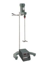
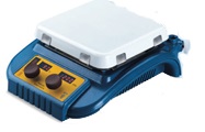
Geared Stirrer (Remi-rqg-128 a/d)
|
The Remi geared stirrer is especially applicable for stirring fluids at a constant rate with a maximum capacity of 8 lts.
It has an 8mm diameter and 450mm long stirring shaft. It gives a speed ranging from 50 to 550 rpm. This is an in-house facility and cannot be borrowed out of the Lab. Use On Payment basis - for details see Forms in http://www.iitk.ac.in/ibc/
|
Location:
|
Ion Beam Complex, NL-105, Department of Physics, IIT Kanpur.
|
Contact:
|
Co-ordinator, IBCOR
Mr. S. Krishnasamy
Technical Superintendent, IBC
(
This email address is being protected from spambots. You need JavaScript enabled to view it.
).
Phone: 7986 / 6993
|
|
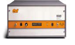
HIGH POWER RF AMPLIFIERS FACILITY
|
The High Power RF Amplifiers (Model 100A250A) facility is present in Microwave Circuit Laboratory at Department of Electrical Engineering IIT Kanpur. The High Power RF Amplifiers 100A250A Amplifier is a self contained, broadband amplifier designed for laboratory applications where instantaneous bandwidth, high gain and moderate power output are required. Utilization of push-pull MOSFET circuitry lowers distortion, improves stability and allows operation into any load impedance without damage. The AR 100A250A Amplifier, when used with an RF sweep generator, will provide a maximum of 100 watts of swept power.
Specifications & Features:
Rated Output Power: 100 watts, Power Output @ 3dB compression (Nominal: 157 watts), Power Output @ 1dB compression (Nominal: 107 watts), Flatness: ± 1.5 dB maximum, Frequency Response: 10 kHz - 250 MHz instantaneously, Gain (at maximum setting): 50 dB minimum, Gain Adjustment (continuous range): 18 dB minimum, Input Impedance: 50 ohms, VSWR 1.5:1 maximum, Output Impedance: 50 ohms, VSWR 2.0:1 maximum. Modulation Capability: Will faithfully reproduce AM, FM, or pulse modulation appearing on the input signal, Remote Interfaces: IEEE-488, RS-232, RF Input: Type “N” female on front panel, RF Output: Type “N” female on front panel.
|
Location:
|
Microwave Circuit Laboratory, Department of Electrical Engineering,
IIT Kanpur
|
Contact:
|
Prof. Kumar Vaibhav Srivastava
This email address is being protected from spambots. You need JavaScript enabled to view it.
|
|
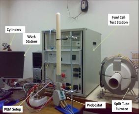
High Temperature Electrochemical Test Station
|
This Instrument is specially designed for testing proton exchange membrane (PEM) fuel cells, and solid oxide fuel cell (SOFC) using the Probostat fixture with maximum temperatures of 800°C. The test stations can be used for characterization of components, the evaluation of SOFC single cells and for optimization of processes. This system is ideal for researchers and developers to begin or expand their testing of Solid Oxide Fuel Cell button cells.
Unique features:
The Test Station provides control of flow (MKS Type 1179A and 2179A Mass-Flo Controller and Type 179A mass-Flo Meter), heating rate, humidity, back-pressure (Maximum 70 psig), temperature (Type T thermocouple) and pressure for the anode and cathode gases. The station incorporates a DC electronic load. The Station also includes two humidity bottles.
-
This station tests single cells and any stack of up to 10 Volts and 100 amps at 150watts maximum power. An electronic load that is programmable through a GPIB/PC interface controls the voltage and current.
-
Safety features include an anode nitrogen purge, an automatic system shutdown of anode and cathode gas streams, humidity bottles and cell heaters.
-
The ProboStat is a cell for measurement of electrical properties, transport parameters etc. It is also used to find the kinetics of materials, solid/gas interfaces and electrodes under controlled atmospheres at high temperatures.
-
The furnace is 3210 Series Split Tube Furnace with dimensions 3-3/4 in. ID x 12 in. OD x 9 in. long. The heating length is 6 in. The material used in manufacturing is Kanthal A1 and the maximum achievable temperature is 1100OC. Power Input required is 230V AC supply.
|
Location:
|
WL210, Department of Materials Science & Engineering,
IIT Kanpur
|
Contact:
|
Prof. Krishanu Biswas
kbiswas@ iitk.ac.in
|
|
High-performance liquid chromatography
|
High-performance liquid chromatography (or high-pressure liquid chromatography, HPLC) is a chromatographic technique that can separate a mixture of compounds and is used to identify, quantify and purify the individual components of the mixture. The HPCL (Varian) (Figure 1) was established in the Environmental Lab in 2010 with the DST grant of the Institute.
Basic Principle:
Separation is based on the analyte’s relative solubility between two liquid phases. HPLC utilizes different types of stationary phase (typically, hydrophobic saturated carbon chains), a pump that moves the mobile phase(s) and analyte through the column, and a detector that provides a characteristic retention time for the analyte. Analyte retention time varies depending on the temperature of the column, the ratio/composition of solvent(s) used, and the flow rate of the mobile phase. With HPLC, a pump (rather than gravity) provides the higher pressure required to propel the mobile phase and analyte through the densely packed column (Figure 2). HPLC – Modes: Normal Phase - Polar stationary phase and non-polar solvent and Reverse Phase - Non-polar stationary phase and a polar solvent.
Unique Features:
Fully integrated, fully automated, modular HPLC pumping systems. With a wide range of flow rates, precise solvent flow and system pressure are maintained with a built-in pressure unit. User-friendly pump heads are self-contained units that can be rapidly exchanged by simply loosening a finger-tight clamp. PEEK and titanium pump heads are available to protect biological samples from trace amounts of metal ions that might be released from components in the fluid path.
|
Location:
|
Department of Chemical Engineering, Environmental Lab,
IIT Kanpur
|
Contact:
|
Prof. Nishith Verma
This email address is being protected from spambots. You need JavaScript enabled to view it.
|
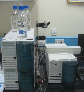
Figure 1
|
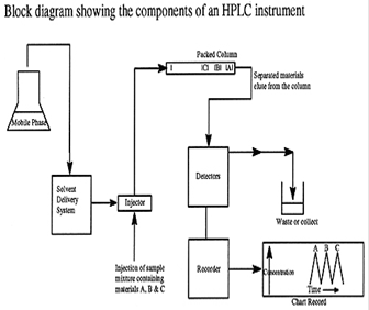
Figure 2
|
Figure 3
|
|
HIGH RESOLUTION ESI-MS (LC-MS) FACILITY
|
Electrospray ionization is a technique used in mass spectrometry to overcome the propensity of macromolecules to fragment (Nobel Prize in Chemistry, 2002).
In ESI, a liquid containing the analyte is pushed through a very small charged metal capillary by a carrier gas. The charge contained in the capillary is transferred to the liquid, which charges the g g p y q , g analyte molecule. As like charges repel, the liquid pushes itself out of the capillary and forms an aerosol of small droplets. A neutral carrier gas is used to evaporate the neutral solvent in the small droplets, this in turn brings the charged analyte molecules closer together. As proximity of the molecules in the droplet becomes lesser and similarly charges molecules come closer together, the droplets explode. This process repeats itself until the analyte is free of solvent and is reduced to lone ions. The lone ions will then continue along to a mass analyzer.
Capability:
ESCI ionisation capability that allows both ESI and APCI to be performed, during one experiment, with the same source.
|
Location:
|
Department of Chemistry
IIT Kanpur
|
Contact:
|
Prof. S. N. Tripathi
This email address is being protected from spambots. You need JavaScript enabled to view it.
|
|
Hot Isostatic Press
|
Hot Isostatic Pressing (HIP) process, subjects a component to elevated temperatures and pressures eliminates internal voids and creates clean, firm bonds and fine, uniform microstructures. The virtual elimination of internal voids helps in designing components to near-net shapes of improved fatigue strength. Generally HIP process enables to produce materials of all shapes and sizes, including cylindrical billets, flat rectangular bar billets, solid shapes with complex external geometry, and complex shapes with internal cavities HIP process provides a method for producing components from diverse powdered materials, including metals and ceramics. During the manufacturing process, a powder mixture of several elements is placed in a container. The container is subjected to elevated temperature and very high vacuum to remove air and moisture from the powder. The container is then sealed and HIP’ed. The application of high inert gas pressures and elevated temperatures results in the removal of internal voids and creates a strong metallurgical bond throughout the material. The result is a clean homogeneous material with a uniformly fine grain size and a near 100% density.
Technical Specification:
Max Pressure: 30,000 psi
Max Temperature: 2200 0C
Environment: Argon gas
Die material: Graphite
|
Location:
|
ACME building, 208
IIT Kanpur
|
Contact:
|
Prof. J.Ramkumar
This email address is being protected from spambots. You need JavaScript enabled to view it.
Prof. Kamal. K. Kar
This email address is being protected from spambots. You need JavaScript enabled to view it.
|
|
Hot Plate (Tarsons- 231b-5040)
|
The Tarsons Hot plate has a 18cmx18cm ceramic top for placing the samples on I for heating. Even beakers can be heated on it.
The temperature can be varied from 100℃ to 1000℃. This is an in-house facility and cannot be borrowed out of the Lab. Use On Payment basis - for details see Forms in http://www.iitk.ac.in/ibc/
|
Location:
|
Ion Beam Complex, NL-105, Department of Physics, IIT Kanpur.
|
Contact:
|
Co-ordinator, IBC
OR
Mr. S. Krishnasamy
Technical Superintendent, IBC
(
This email address is being protected from spambots. You need JavaScript enabled to view it.
).
Phone: 7986 / 6993
|
|
iCAP 6300 ICP Spectrometer
|
The use of Inductively Coupled Plasma source (ICP) and Atomic Absorption (AA) are the accepted and most powerful techniques for the analysis of and quantification of trace elements in both solid and liquid samples. Applications range from routine environmental analyses to the materials industry, geological applications to clinical research and from the food industry to the semiconductor industry. The iCAP 6300-Duo can simultaneously detect 66 Elements with detection limits less than 1μg/L. The plasma is easier to ignite and can operate with a much wider range of sample types. The Duo instrument provides flexibility, with extreme detection limits achievable in axial mode and reduced interference in Radial mode.
|
Technical Specification
|
|
|
Spectrometer
|
Echelle type
|
| |
52.91 grooves/mm ruled grating
|
| |
383 mm effective focal length
|
| |
9.5 0UV fused silica cross dispersion prism
|
|
Wavelength range
|
166 – 847 nm
|
|
Spectral bandpass
|
7 pm at 200 nm
|
|
Detector
|
High performance CID86 Chip
|
|
RF source
|
27.12 MHz solid state
|
| |
750 – 1500 watts output power
|
| |
(Duo restricted to 1350 watts)
|
|
Sample Pump
|
3 – channel, 12 roller peristaltic.
|
| |
Speed 0 -125 rpm
|
|
Plasma gas
|
Fixed 12 L/min, argon
|
|
Nebulizer gas
|
Pressure control, form 0 - 0.4 Mpd
|
|
Auxiliary gas
|
4 fixed flows, 0, 0.5, 1.0 and 1.5 L/min
|
|
Standard sampling kit
|
Concentric glass nebulizer
|
| |
Glass cyclone spray chamber
|
| |
Semi – demountable torch
|
| |
1.5 mm bore quartz injector (radial version)
|
| |
2 mm bore quartz injector (Duo version)
|
|
Dimensions
|
840 W* 750 D *590 H
|
|
Location:
|
Department of Civil Engineering,
IIT Kanpur
|
Contact:
|
Prof. Tarun Gupta,
This email address is being protected from spambots. You need JavaScript enabled to view it.
|
Figure 1
|
|
Imaging Spectroscopic Ellipsometer
|
Ellipsometry is a well-known non-destructive optical method for determining film thickness and optical properties. Imaging Ellipsometry combines the power of ellipsometry with microscopy. The EP³-SE offers greatest flexibility for measurements with Imaging Ellipsometry. It allows the analysis of multilayer/multi parameter systems and to choose a proper wavelength for absorbing materials. Additionally, a multiple- wavelengths mapping of the field of view (Micro- Mapping) is possible, yielding thickness and/or refractive index maps – similar to AFM surface topographies. For each wavelength the highest available lateral resolution can be achieved, which makes the EP³-SE to a unique instrument for spectroscopic measurements of micro- structured samples. The spectroscopic Imaging Ellipsometer EP³-SE uses a Xenon arc lamp to address up to 46 wavelengths between 365 nm to 1000 nm.
|
Location:
|
Thematic Unit of Excellence,
IIT Kanpur
|
Contact:
|
Prof. Ashutosh Sharma
This email address is being protected from spambots. You need JavaScript enabled to view it.
Dr. Prabhat Dwivedi
This email address is being protected from spambots. You need JavaScript enabled to view it.
Dr. Dinesh Deva
This email address is being protected from spambots. You need JavaScript enabled to view it.
|
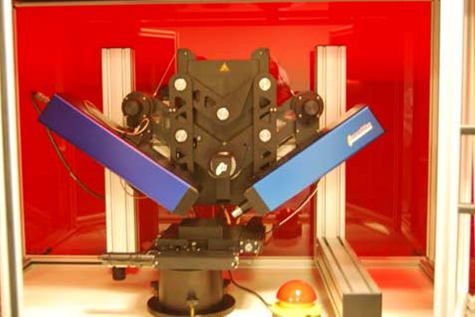
|
INSTRUMENT FOR DIFFUSE LIGHT MEASUREMENTS: ISS IMAGENT
|
This instrument, Imagent manufactured by ISS*, is used to detect diffuse light to characterize random media. Its working principle is based on the use of near infrared light for probing random media such as tissue, brain activities through the cortical surfaces, etc. The light passing through tissue is either absorbed or scattered. In the near infrared region (650-950 nm wavelength), a measurable amount of light can pass through due to the reduced absorption associated with hemoglobin and water, thus making the photon propagation dominantly scattering/diffusive. Light from modulated sources is carried through optical fibers and the scattered light is measured via optical fiber bundle with a photomultiplier tube (PMT) detector. Such measurement can be used to obtain clinically important information of the tissue such as the absorption and scattering coefficients and the hemoglobin concentrations. A data acquisition program called Boxy is available, which measures and records frequency-domain measurement parameters (AC, DC, Phase) as a function of light source number and time. In order to calculate the value of the absorption and scattering coefficients and hemoglobin concentration from the recorded data set, user may include his/her own choice of User Calculation Libraries (user written dynamic link libraries). The system does not create tomographic image of the random media. We are developing algorithms to undertake diffuse light tomography of random media.
INSTRUMENT SPECIFICATIONS :
-
Modulation frequency 110 to 300 MHz.
-
Eight laser-diode sources, four of wavelength 690nm and another four of 830nm.
-
Two photomultiplier tube (PMT) based detectors.
-
Light source optical power is about 1mW average.
-
The PMTs are sensitive to pW power levels.
-
Multiplexing scheme: detectors time shared by turning sources on and off in fast cycles.
-
All fiber-optic coupled
Light source fibers – 400 micrometers core.
Light detectors fiber – 3 mm diameter bundle.
|
Location:
|
Department of Physics
IIT Kanpur
|
Contact:
|
Harshawardhan Wanare
This email address is being protected from spambots. You need JavaScript enabled to view it.
|
ISCO Density Gradient Systems
|
Density gradient centrifugation is used for density based gentle isolation of cellular ribosomes, RNA, DNA, organelles or any other component. ISCO Density Gradient Systems automate the preparation of gradients, fractionation and UV scanning of zones after the centrifugation. This Programmable Density Gradient System reproducibly forms density gradients and Samples can be immediately loaded on-to prepared gradients and spun in a centrifuge. Once the centrifugation is completed, the system allows you to fractionate and quantitate different zones formed due to centrifugation with high precision. The Isco Density Gradient System produces a continuous absorbance profile as the gradient is collected in precisely measured fractions. Fractionation is performed by introducing a dense chase solution into the bottom of the centrifuged tube, raising the gradient intact by bulk flow. Chase solution may be injected either by piercing the bottom of the tube or from the top with the optional cannula.
Applications:
-
Protein interactions
-
Separation of organelles
-
Separation of mRNA, DNA
-
Cell synchronization
-
Protein isolation
-
Nucleic acid isolation
Features of the machine-
-
System includes tube piercing stand; peristaltic pump; UA-6 Detector with 254 and 280nm filters, density gradient flow cell; Foxy Jr. Fraction Collector, Gradient Former, organizer shelf, cables, and tubing
-
Prepare gradients and use immediately without overnight refrigeration.
-
Hands-off fraction separation; rack for collection in microcentrifuge tubes
-
Seals and punctures the bottom of most common centrifuge tubes.
-
Zone broadening and mixing are minimized with upward bulk flow.
-
254 and 280 nm detector wavelengths included.
|
Location:
|
Department of Electrical Engineering,
IIT Kanpur
|
Contact:
|
Prof. A. R. Harish
This email address is being protected from spambots. You need JavaScript enabled to view it.
|
|
I-V Measurement system
|
The Current –Voltage measurement system comprises of a Keithley Source Meter (model 6430), with a convenient DMM interface, and with I-V measurement capability ranging from 1100V to 10nV and 10.5A to 1fA.
General current and voltage measurements can also be obtained in the range mentioned above. This is an in-house facility and cannot be borrowed out of the Lab. Use On Payment basis - for details see Forms in http://www.iitk.ac.in/ibc/
|
Location:
|
Ion Beam Complex, NL-105, Department of Physics, IIT Kanpur.
|
Contact:
|
Co-ordinator, IBC
OR
Mr. S. Krishnasamy
Technical Superintendent, IBC
(
This email address is being protected from spambots. You need JavaScript enabled to view it.
).
Phone: 7986 / 6993
|
|
Laser Induced Incandescence (LII) - Instrument for Soot Characterization
|
Procures in the Financial Year: 2010 -11
Laser-induced incandescence is an optical technique for accurate, non-intrusive, and temporally resolved measurement of soot concentration, specific surface area and primary particle diameter
|
Specification:
|
All measurements
|
|
Sampling Frequency:
|
20Hz
|
Concentration:
|
|
Low end
|
<1part per trillion
|
| |
<2 micrograms/cubic meter
|
|
High End
|
10 parts per million
|
| |
20 grams/cubic meter
|
|
Range
|
>1,000,000:1
|
|
Precision
|
+/ -2%
|
Primary Particle Size:
|
|
Range
|
10 - 100 nm
|
|
Precision
|
+/- 2%of max
|
|
Specific Surface Area:
|
50 - 200 M2/g
|
|
Location:
|
Flame Dynamics Lab, FDL-T101, Department of Aerospace Engineering,
IIT Kanpur
|
Contact:
|
Prof. Abhijit Kushari
This email address is being protected from spambots. You need JavaScript enabled to view it.
|
User Charges: :
|
Free
|
|
|
Laser Micromachining
|
The laser micromachining (LMM) equipment can be used for engraving and creating micro-features in metallic substrates. The parts to be removed are locally vaporized using Nd:YAG laser and that vapor can be sucked with a vacuum pump. The laser micromachining equipment (V3+, laservall, Italy) is established in the Western Lab from a DST grant for the micro-fabrication lab.
Basic Principle:
The basic principle is similar to that of laser spot welding. The only difference is that in this equipment the mirror 3 and lens 4 are moved in such a way that the spot 5 can be moved to the required position.
Unique Features:
Features ranging from 50 μm to 1mm can be created very easily. The shapes that are difficult to manufacture using conventional machining can be created easily using LMM equipment.
|
Location:
|
Department of Chemical Engineering,
IIT Kanpur
|
Contact:
|
Prof. Deepak Kunzru
This email address is being protected from spambots. You need JavaScript enabled to view it.
|
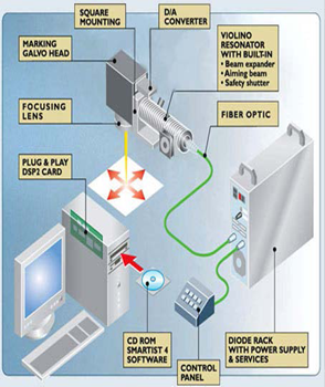
Figure: 1
|
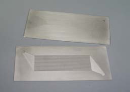
|
Laser Spot Welding Equipment
|
The laser spot welding (LSW) equipment can be used for welding small-sized, metal materials. The parts to be joined are locally melted using Nd:YAG laser and fused together. The laser spot welding equipment (Mastercubo 60, laservall, Italy) is located in the Western Lab and has been established from a DST grant for the micro-fabrication lab.
Basic Principle:
The physical principle of laser weld uses a beam of electromagnetic waves in phase, photons focalized with optical mediums and concentrated on the piece creating high powers. When beam shoots the surface the energy is partially reflected and partially absorbed causing the fusion of the material. If the concentration exceeds a certain limit there’s instantaneous vaporization of the base metal in the zone where the beam is more concentrated, in the zone around, instead, there’s melted metal. Metallic vapour at high temperature and pressure pushes laterally the melted and the beam proceeds in the below metal. The hole created is defined as a keyhole. Equilibrium is created between the vapor pressure that wants to enlarge the hole and the hydrostatic pressure of the melted metal that wants to close the hole. This equilibrium determines the penetration depth of the hole in the work piece.
The optical mechanism can be described as follow (please refer to Fig. 2):
-
The laser beam emerges from optical fiber 1
-
Lens 2 align the laser beam on mirror 3
-
Mirror 3 turns the laser beam on the focusing lens 4
-
Lens 4 focuses the laser beam on 5
Unique Features:
Because of the small spot size resulting due to the thin laser beam, one can very easily adopt this technique for joining two thin plates of thickness around 1 mm.
|
Location:
|
Department of Chemical Engineering,
IIT Kanpur
|
Contact:
|
Prof. Deepak Kunzru
This email address is being protected from spambots. You need JavaScript enabled to view it.
|
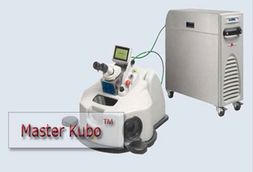
Figure : 1
|
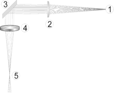
Figure : 2
|
Figure : 3
|
|
Leica Microscope
|
Optical microscopy is the oldest and most utilized method for microstructural evaluation of materials. Optical Microscopy uses the geometry and refractive indices of transparent optics to focus light and induce a magnification. The optical microscope (Leica DM2500 M) is established in the Western lab from a DST grant for the micro-fabrication lab.
Basic Principle:
The objective lens is, at its simplest, a very high powered magnifying glass i.e. a lens with a very short focal length. This is brought very close to the specimen being examined so that the light from the specimen comes to a focus about 160 mm inside the microscope tube. This creates an enlarged image of the subject. This image is inverted and can be seen by removing the eyepiece and placing a piece of tracing paper over the end of the tube. By carefully focusing a brightly lit specimen, a highly enlarged image can be seen. It is this real image that is viewed by the eyepiece lens that provides further enlargement.
Unique Features:
Fully integrated and fully automated x, y and z direction stage. Fluorescence bulb is also attached for biological applications. Up to 20X magnification.
|
Location:
|
Department of Chemical Engineering,
IIT Kanpur
|
Contact:
|
Prof. Deepak Kunzru
This email address is being protected from spambots. You need JavaScript enabled to view it.
|
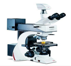
Figure: 1
|
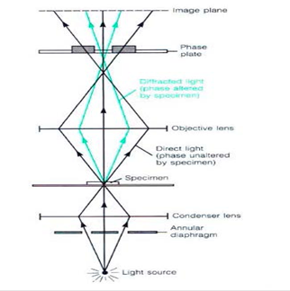
|
Leica CM 1900 Cryostat
|
Leica CM1900- configuration 4 with cryochamber and specimen cooling with specimen retraction and specimen orientation. Freestanding cryostat with encapsulated, spash proof microtome. Single-screw locking system for direct fitting of specimen discs. Twin Compressor cooling system for cryochamber and specimen head. Cryochamber temperature setting between 0 and -35 C.
Technical Specifications:
-
Operating voltage 230V\50Hz, Section thickness continuously adjustable from 1 to 60 micrometers, total vertical stroke approx. 60mm, total horizontal specimen feed approx. 25mm, motorized coarse feed at 0.8mm/s speed, LED display for cryochamber and specimen head temperature, actual time, defrost time, visual indication of specimen stop position, Cryochamber temperature setting between 0 and -35 C, specimen temperature control between -10 and -50C
-
360o manually rotatable λ/2 plate achromatic for wavelength 450 to 700nm, Polarization filter wheel for X1 port.
|
Location:
|
Biomedical Optics and Spectroscopy Laboratory, SL-111, Department of Physics
IIT Kanpur
|
Contact:
|
Prof. Asima Pradhan
This email address is being protected from spambots. You need JavaScript enabled to view it.
|
|
Magnetic Stirrer ( Spinit-231a)
|
The Spinit Magnetic stirrer is a motor-less stirrer. Liquids up to 750 ml can be placed in glass beakers over the stirrer platform, and can be stirred using magnetic stirring capsules of various sizes, placed inside the beaker at the bottom. The stirrers are Teflon coated to prevent corrosion and to avoid contamination of the solution being stirred. This is an in-house facility and cannot be borrowed out of the Lab. Use On Payment basis - for details see Forms in http://www.iitk.ac.in/ibc/
|
Location:
|
Ion Beam Complex, NL-105, Department of Physics, IIT Kanpur.
|
Contact:
|
Co-ordinator, IBC
OR
Mr. S. Krishnasamy
Technical Superintendent, IBC
(
This email address is being protected from spambots. You need JavaScript enabled to view it.
).
Phone: 7986 / 6993
|
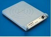
|
Micro Tribometer Facility
|
Wear of materials is one of the most important causes of failure of components like acetabular cup and ball etc. A detailed study of the principles of friction, wear and lubrication i.e. the tribological properties, is necessary to certify a material as a potential body implant. With the above intention a pin on disk tribometer set-up (Fig. 1) was procured from Nanovea Inc. USA.
Unique features:
Following are the main features of the micro tribometer:
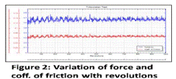
-
Continuous force vs. coefficient of friction plot (Fig. 2)
-
Depth sensor based on white light instead of laser that provides much more accurate depth profile of worn sample
-
Speed from 0.1 to 2000 rpm
-
Provides three lubrication modes: Using a low pressure pulverization module, air is compressed and filtered then mixed with liquid to create a uniform spray that can be directed to the appropriate test zone.
-
A drop by drop lubrication with flow control
-
The soak option performs friction tests and wear tests under fluid in a specialized cup surrounding sample holder, allowing full submersion of the sample.
|
Location:
|
Biomaterials Processing & Characterization Laboratory
(behind Western Laboratories).
IIT Kanpur.
|
Contact:
|
Prof. Kantesh Balani,
This email address is being protected from spambots. You need JavaScript enabled to view it.
|
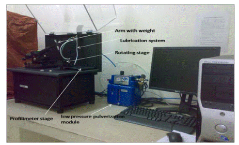
|
Microanalysis
|
Microanalysis is the most important chemical analysis that is required for organic, inorganic and organometallic compounds. This is a basic and important facility that gives valuable primary information of the composition of a chemical compound, i.e., various elements present in the compounds. Using this method, normally the percentage of elements, such as C, H, N, S / O present in the organic compounds can be obtained experimentally. This technique is based on the combustion process where the sample (~1-2 mg) is heated to high temperature in the presence of oxygen atmosphere. The oxidized and the reduced volatiles, such as CO2, H2O and N2, have been absorbed using different traps separately and the quantity of the gases absorbed is measured using the detectors (Charts 1 and 2). From this the values of the C, H, and N present in the organic compounds can be found. Although this method has been known widely for the organic compounds, nowadays, metal-organic, organometallic, and the coordination compounds have also been used for the measurements of the C, H, and N elemental composition.
This instrument has the following features: C, H, and N can be measured simultaneously
S and O can be measured separately
10 – 30 mg is required for the analysis
Analysis time is 15 min. per sample.
All kinds of solid and liquid samples can be analyzed
The accuracy and precision is < 0.3 % (+ 0.15%)
|
Location:
|
Core lab, no. CL-107C, Department of Chemistry,
IIT Kanpur
|
Contact:
|
V. Chandrasekhar
This email address is being protected from spambots. You need JavaScript enabled to view it.
|
Microsystems Fabrication Laboratory
|
The Microsystems laboratory has been commissioned within the Department of Mechanical Engineering in the year 2009-2010 by the financial support provided by the institute CARE program and through the external merit based funding that has been obtained by the Principle investigator and Co-PI of this CARE proposal. The laboratory has been commissioned with the following vision:
Vision of the Laboratory:
Our Long term vision is to establish a working micro-engineering center for excellence in functional micro-scale prototypes. The goal is to promote basic MEMS research and training, developing MEMS sensor modules for commercial and futuristic applications, generate resources for the institute through grant proposals, sale of patented technologies and developing MEMS educational modules. The bigger objective of this center is to develop the 21st century engineering and technical task force who would take up the technological challenges of the future decades
|
Location:
|
NET building, Department.of Mechanical Engineering,
IIT Kanpur
|
Contact:
|
Prof. Shantanu Bhattacharya
This email address is being protected from spambots. You need JavaScript enabled to view it.
|
Microwave Sintering Facility
|
Unlike ceramics, sintering of metal powder compacts necessitates the need of controlled atmosphere cavity. For conducting such an experiment, a 1.1 kW microwave furnace with a 2.45 GHz multi-mode cavity was indigenously designed and established at Powder Metallurgy Laboratory, IIT Kanpur, in collaboration with Bharat Heavy Electrical Ltd. (BHEL), Hyderabad, India. The detailed description of the furnace [model:Sinterwave] construction has already been patented [Tubular Microwave Sintering Furnace with Inert and Reducing Gas Flushing for Sintering Metallic Samples, A. Upadhyaya (IIT/K) and G. Swaminathan (BHEL) Patent No. 1147/DEL/2006, Publication Date: 23.11.2007]. Figures 1and 2 illustrate the different parts of the microwave furnace facility and the schematic of the entire setup, respectively.
Unique features:
The size of the metallic cavity was 40 × 62 cm. A high density (99.9%), doubly recrystallized alumina tube of 7.1 cm diameter and 67 cm in length was positioned at the center of the furnace. All the sintering experiments for metallic powder compacts are usually conducted in hydrogen. The full-density alumina tube prevents any gas leakage. Furthermore, pore-free alumina is transparent to microwaves and does not heat up. Thus, the temperature rise during sintering is solely due to microwave-metal interaction. An insulation package made of Fibrefrax TM boards was used to surround the tube at the center of the cavity to minimize heat loss. The design was so made that it could be used both with and without the use of suscept or secondary coupler. The sintering studies can be conducted using SiC plates. The temperature measurement is carried out using an infrared pyrometer (model: M680, supplier: Mikron Inc., USA). The infrared pyrometer output was coupled with a PC based data acquisition and display software.
|
Location:
|
Powder Metallurgy Laboratory, Department of Materials and Metallurgical Engineering,
IIT Kanpur
|
Contact:
|
Prof. Anish Upadhyaya
This email address is being protected from spambots. You need JavaScript enabled to view it.
|
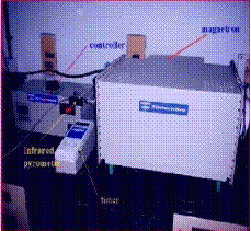
|
|
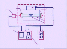
|
|
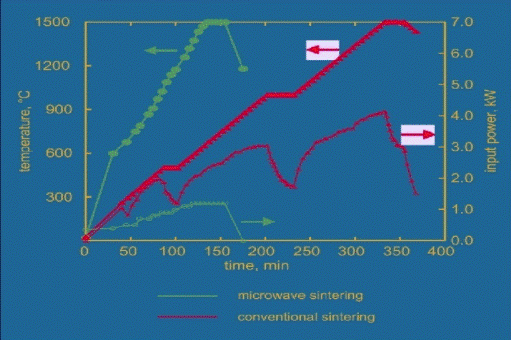
|
Mask less Photolithography
|
The SF-100 is an elegantly simple, easy to use micro patterning system. Through its unique patented design, the system allows user to fabricate micro-devices quickly and easily. It is capable of fabricating 15 μm features over 1.7 cm2 area, and 5 μm features over 0.2 cm2 area. Very complex structures can easily be fabricated just by drawing a bitmap image on the computer screen. Gray scale photolithography allows the fabrication of complex Micro-fluidic devices in a single step.
|
Location:
|
Thematic Unit of Excellence,
IIT Kanpur
|
Contact:
|
Prof. Ashutosh Sharma
This email address is being protected from spambots. You need JavaScript enabled to view it.
Dr. Prabhat Dwivedi
This email address is being protected from spambots. You need JavaScript enabled to view it.
Dr. Dinesh Deva
This email address is being protected from spambots. You need JavaScript enabled to view it.
|
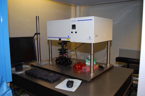
|
MICRO TRIBOMETER FACILITY (Pin-on-Disk ASTM G99)
|
Wear of materials is one of the most important causes of failure of components like acetabular cup and ball etc. A detailed study of the principles of friction, wear and lubrication i.e. the tribological properties, is necessary to certify a material as a potential body implant. With the above intention a pin on disk tribometer set-up (Fig. 1) was procured from Nanovea Inc. USA.
Unique features:
Following are the main features of the micro tribometer:
-
Continuous force vs. coefficient of friction plot (Fig. 2)
-
Depth sensor based on white light instead of laser that provides much more accurate depth profile of worn sample
-
High Resolution non-contact 3D Profiler provides the profile of the wear track
-
Software create 3D imaging of the wear track
-
Vertical Resolution down to a few nanometers (~10 nm) and lateral resolution down to 1 μm are possible (Fig. 3)
-
Speed from 0.1 to 2000 rpm
-
Provides three lubrication modes:
-
Using a low pressure pulverization module, air is compressed and filtered then mixed with liquid to create a uniform spray that can be directed to the appropriate test zone.
-
A drop by drop lubrication with flow control
-
The soak option performs friction tests and wear tests under fluid in a specialized cup surrounding sample holder, allowing full submersion of the sample
|
Location:
|
Biomaterials Processing & Characterization Laboratory, Department Of Materials Science & Engineering,
IIT Kanpur
|
Contact:
|
Prof. Kantesh Balani
kbalani@ iitk.ac.in
|
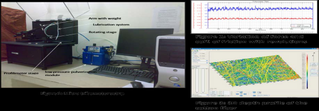
|
Multi modal Information Processing Systems (MiPS) Lab
|
The Multi modal Information Processing Systems Lab was established in 2008 at the Department of Electrical Engineering with grants from IIT Kanpur and other funding agencies.
Theme:
The focus of the Lab infrastructure is to create intelligent environments in which humans and machines (i.e., equipments, rooms, and structure) collaborate with each other in a seamless manner and to deliver the information to the user desiring such an information in linguistic and visual modalities. Hence a transformation of the signal to higher-level semantic information for interpretation is required. For example, a meeting room, an entire building, can be converted to an intelligent environment. To incorporate the functionalities described above, development of the necessary theories, algorithms, and implementation prototypes is quintessential and is the goal of research at MiPS Lab. The primary focus of research currently is on multi-modal (speech, audio, video and text) processing.
Infrastructure :
The Lab has a multi channel audio-visual data acquisition test bed which can record upto 32 channels of synchronized multi-modal data. The test bed can also acquire additional modalities like handwriting, haptic inputs. Figure 1, illustrates a photograph of the test bed being used as a meeting room. Figure 2, gives a schematic of the facility. The test bed is also equipped with high fidelity electret microphones and high resolution cameras capable of distant speech, audio and video signal acquisition. Figure 4, illustrates the computing infrastructure at MiPS Lab. It is equipped with the state of the art data server and three industry grade voice servers based on the open source asterisk software. The voice servers are connected to both analog and digital (ISDN-PRI ) lines capable of handling multiple simultaneous audio and video calls. Figure 3 illustrates an intelligent video retrieval application hosted on this infrastructure.
|
Location:
|
Department of Electrical Engineering,
IIT Kanpur
|
Contact:
|
Prof. Rajesh Hegde
This email address is being protected from spambots. You need JavaScript enabled to view it.
|
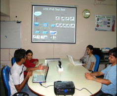
Fig: 1
|
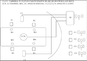
|
|
Multilayer PCB Press Machine
|
For fabricating multilayer PCB we have to first fabricate corresponding number of double sided PCBs. For 4 layer PCB we have to first fabricate two double layer PCBs. Similarly for 6 layer PCB, 3 double layer PCBs are to be fabricated.
These double layer PCBs are sandwiched one over another exactly with oxidizing agent between them. Then it is inserted in multilayer press machine. It has control unit for pneumatic pressure supply, press plates and heaters. The unit is controlled by two digital and adjustable thermostats, one digital timer as well as a pressure valve with pressure meter. Two strong air ventilators activated automatically during cooling cycle.
After complete curing and cooling of PCB, the PCB is taken out from the press machine and it is subjected for masking and legend printing as per requirement
|
Location:
|
PCB Fabrication Laboratory, of Electrical Engineering,
IIT Kanpur
|
Contact:
|
Prof. Shyama Prasad Das
This email address is being protected from spambots. You need JavaScript enabled to view it.
|
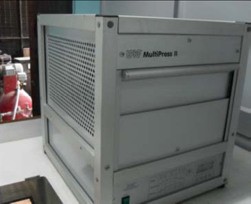
|
Nano Cal-C
|
The Nano Cal-c is a thin film measurement instrument which is capable of measurement of stacks of transparent films up to 500nm. It is based on the principle of reflectance measurements carried out by a laser and detector.
|
Location:
|
NET building, Department.of Mechanical Engineering
IIT Kanpur
|
Contact:
|
Prof. Shantanu Bhattacharya
This email address is being protected from spambots. You need JavaScript enabled to view it.
|
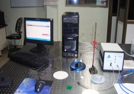
|
NMR (400 Mhz) Spectrometer
|
The Nuclear Magnetic Resonance spectroscopy is vital for both organic and inorganic chemists for structure elucidation on a routine basis and to follow reactions and dynamic chemical events on a real time scale. The state-of-the-art JEOL 400 MHz spectrometer, funded by IRPHA-DST in 1998, was installed in the Department of Chemistry during March 1999. Through CARE funding from IIT Kanpur, the machine was equipped with an auto-sampler in 2005. This augmentation has facilitated the use of the machine round the clock. On average, 60-80 spectra/day have been recorded since its installation. The facility has been of tremendous utility for well over 100 research students working in diverse areas of organic and inorganic chemistry within the department as well as others within and outside of IITK, for example HBTI, Gorakhpur University, DRDO Labs etc. .
Unique features:
-
The autotune function allows tuning of various frequencies with a computer control. This facilitates a variety of NMR-active nuclei such as 1H, 13C, 19F in distinct chemical environments to be probed without any time delay.
-
Because of high resolution, a number of 2- and 3-dimensional NMR spectral acquisition can be readily carried out.
-
The low-temperature accessory permits variable-temperature (VT) NMR studies to be performed. d) The high resolution allows a variety of magnetic measurements to be performed.
|
Location:
|
Core Labs, Department of Chemistry,
IIT Kanpur
|
Contact:
|
Prof. J. N. Moorthy
This email address is being protected from spambots. You need JavaScript enabled to view it.
|
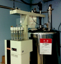
|
|
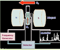
|
|
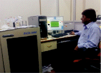
|
Nano-Imprint Lithography
|
Eitre allows replication of patterns in the micro- and nanometer range. It offers a complete range of imprint methods, including thermal NIL, hot embossing, UV NIL, as well as Obducat's proprietary Simultaneous Thermal and UV (STU®) imprint process. All Nano Imprint Lithography (NIL) systems from Obducat are equipped with full area thermal imprint, using the patented Soft Press® technology. The proprietary design of the heater, embedded in the substrate chuck, provides a homogeneous temperature distribution across the whole imprint area. The uniform heating and a wide range of temperature settings, makes it possible to use a wide range of imprint polymer. The proprietary Simultaneous Thermal and UV (STU®) technology enables simultaneously combined thermal and UV nano imprint lithography, allowing the complete imprint sequence into UV-curable thermoplastic pre-polymers to be performed at a constant temperature.
|
Location:
|
Thematic Unit of Excellence,
IIT Kanpur
|
Contact:
|
Prof. Ashutosh Sharma
This email address is being protected from spambots. You need JavaScript enabled to view it.
Dr. Prabhat Dwivedi
This email address is being protected from spambots. You need JavaScript enabled to view it.
Dr. Dinesh Deva
This email address is being protected from spambots. You need JavaScript enabled to view it.
|
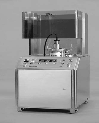
|
NT-1100 WYKO Optical Profiler
|
3-dimensional images of surfaces and structures, Two measurement techniques: vertical scanning interferometry (VSI, rough samples) and phase shift interferometry (PSI, smooth samples), Vertical resolution better than 1 nm and horizontal resolution better than 400 nm, Objectives of 5x and 50x, intermediate lenses of 0.5x, 1x and 2x. The combination of both allows us to measure surfaces areas from 1mm2 to 60mm2. Working principle: White light interferometric microscopy.
Special features:
Basic System Consist of with the following standard components: (1) NT1100 stand with course focus adjustment, (2) 1mm scan range, (3) Dell Pentium PC with Windows XP, (4) 1x FOV lens, (5) Alignment FOV lens, (6) Integrated 5" live video monitor, (7) 30 fps high speed camera, (8) Vision software platform.
|
Location:
|
Optoelectronics Laboratory, Department of Electrical Engineering,
IIT Kanpur
|
Contact:
|
Prof. Utpal Das
This email address is being protected from spambots. You need JavaScript enabled to view it.
|
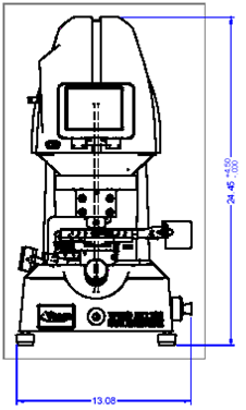 Fig: 1 Fig: 1
|
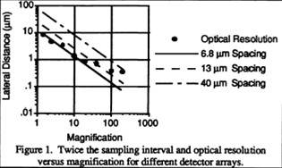
Fig: 2
|
 Fig: 3 Fig: 3
|
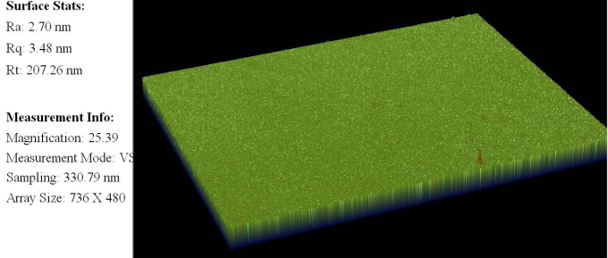
|
Optical Distributed Sensor Interrogator
|
Procures in the Financial Year: 2011-12Model A50 from Luna Technologies
The Luna ODiSI enables high resolution distributed temperature and strain measurements using simple, unaltered, telecom-grade optical fiber as the sensor. With 50 meters maximum sensing length and sub-centimeter spatial resolution, the ODiSI is the paramount tool for
-
Load/fatigue/structural/mechanical testing,
-
Model and simulation validation,
-
Structural health monitoring,
-
Stress profile in foundation and
-
Stress and temperature profile in pavement and foundations,
-
Composite testing.
|
Key features include
|
-
+/- 15,000 microstrain, up to 300O C
-
+/- 1 microstrain, +/- 0.1OC
-
Sub-cm spatial resolution
-
Sampling rate 1 Hz for 50m interrogator and 3 Hz for 10m interrogator
-
Easily deployable, inexpensive sensors
-
1000s of sensing points in a single fiber
-
Disposable/easily replaceable
-
Reduced installation time and cost
-
User configurable gauge length and sensing locations
-
Point and/or distributed sensing anywhere in your device or structure under test
-
Temperature and/or strain in the same sensing fiber
-
Intuitive touch to define sensing points and regions
-
Standard GUI and user customizable software development kit
-
Simple monitoring and data logging
|
Location:
|
Structural Engineering Laboratory, Advance Monitoring and Sensing Room
S-Lab-STL 1, Department of Civil Engineering
IIT Kanpur
|
Contact:
|
Prof. Samit Ray Chaudhuri
This email address is being protected from spambots. You need JavaScript enabled to view it.
Mr. Kunwar K. Bajpai
This email address is being protected from spambots. You need JavaScript enabled to view it.
|
User Charges: :
|
Cost of the fibre will be charged
|
|
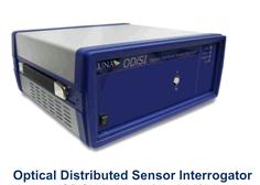
|
|
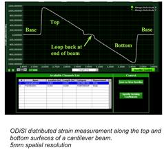
|
Optical Table
|
A rigid horizontal bar or track for holding optical devices in experiments; it allows device positions to be changed and adjusted easily. The vibration isolation table is used along at the base for prevention of vibration transmission to the optical setup kept over this.
|
Location:
|
NET building, Department.of Mechanical Engineering
IIT Kanpur
|
Contact:
|
Prof. Shantanu Bhattacharya
This email address is being protected from spambots. You need JavaScript enabled to view it.
|
|
Oxidation Furnace
|
Thermal oxidation is a simple route to cover a silicon substrate with oxide. In micro devices oxide may be used for a variety of purposes from chemical attachment and modifiability of surfaces to using oxide as a filler material in gaps etc. in microfluidic channels with submicron accuracy level or making micro cantilevers. Based on the type of oxidation thermal oxide may be categorized as dry and wet oxides. In dry oxidation pure oxygen reacts with silicon at high temperatures from 800 deg. C to about 1200 deg. C.
|
Location:
|
NET building, Department.of Mechanical Engineering
IIT Kanpur
|
Contact:
|
Prof. Shantanu Bhattacharya
This email address is being protected from spambots. You need JavaScript enabled to view it.
|
|
Oxford Plasma ICP Etching System. (Plasmalab80 plus)
|
The Plasmalab80Plus is ideally suited to R&D or small-scale production, with 240 mm diameter table allowing 200 mm (8”) wafer or 9 x 50 mm (2”) batch capacity. The open-load design allows fast wafer loading and unloading, ideal for research, prototyping and low-volume production. ICP-RIE cryo process. The electrostatic shield design in the Plasmalab80Plus ICP configuration avoids energetic ion bombardment and capacitive coupling, providing low substrate damage, with long life for the ICP tube and reduced maintenance. The Chemistry used at present is Methane + Hydrogen + Argon with Oxygen for cleaning.
Special features:
On the Plasmalab80Plus, substrate backside cooling, for optimum temperature control is done by a chiller at 20C
|
Location:
|
Optoelectronics Laboratory, Department of Electrical Engineering,
IIT Kanpur
|
Contact:
|
Prof. Utpal Das
This email address is being protected from spambots. You need JavaScript enabled to view it.
|
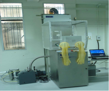
Fig: 1
|
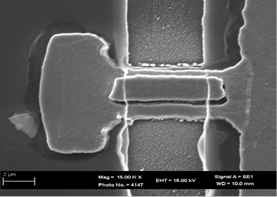
Fig: 2
|
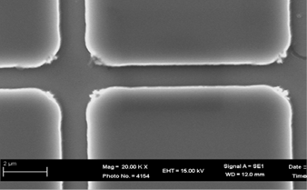
|
Optical Microscope
|
Nikon Eclipse TE2000U is an advanced inverted microscope used for variety of applications which require high precision e.g. live cell microscopy, flow visualization within microfluidic channels, for characterizing interfaces in the area of contact mechanics and so on and so forth.
Features:
The microscope has the facility for standard applications in phase contrast, dark-field and DIC. The microscope has a manual XY stage and motorized Z-focus with an accuracy of50nm. The motor can be operated using a remote control pad. The microscope has DIC & epi-fluorescence attachment for fluorescence microscopy. It has condenser with modules for phase contrast. Available filters are: day colour balance, heat absorbing, green interference and the fluorescence band-pass filter. The microscope has objectives with magnifications: 4X, 10X, 20X and 40X. Many of these features can be further extended
|
Location:
|
Department of Chemical Engineering
IIT Kanpur
|
Contact:
|
Prof. Animangsu Ghatak
This email address is being protected from spambots. You need JavaScript enabled to view it.
|
|
Partial Discharge Detector and Analyser
|
The Partial Discharge Detector and Analyser is available at Department of Electrical Engineering, IIT Kanpur. This facility is currently installed in High Voltage Laboratory. The measurement of partial discharges constitutes an important non-destructive test to gauge the condition of electrical insulation in electrical apparatus.
Unique Features:
The partial discharge intensity is measured in Pico-coulombs (pC) or, alternatively, radio interference voltage (RIV) in microvolts (μV). The partial discharge/RIV measuring system consists of, Partial discharge meter (Type DTM) which is the basic measuring unit with built-in oscilloscope. It has provisions for direct measurement as well as bridge measurement. The basic noise level of the instrument is less than 0.6 pC in the most sensitive measuring range. The measuring accuracy and linearity correspond to IEC 60 270 and IS 6209. The partial discharge intensity measurement ranges from 2 pC to 50,000 pC (IEC 60 270) and radio interference voltage measurement ranges from 1 V to 25,000 mV (VDE, CISPR).
|
Location:
|
High Voltage Laboratory, Department of Electrical Engineering,
IIT Kanpur
|
Contact:
|
Prof. Nandini Gupta
This email address is being protected from spambots. You need JavaScript enabled to view it.
|
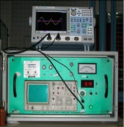
Fig: 1
|
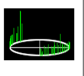
Fig: 2
|
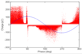
Fig: 3
|
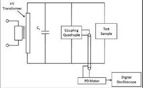
Figure: 4
|
PCB CAD System
|
The software used in PCB lab. is Altium. Altium 2009 was procured for designing and fabricating the PCBs. We are using it, because it is a powerful tool in designing PCB layout. It has enhanced features like improved interactive routing, user selectable track width, internal routing loops, PCB routing completion detector, preserving track angles while dragging, designing bottom layer layout (mirror has to done) just by flip and editing the board etc.
|
Location:
|
PCB Fabrication Laboratory, of Electrical Engineering,
IIT Kanpur
|
Contact:
|
Prof. Shyama Prasad Das
This email address is being protected from spambots. You need JavaScript enabled to view it.
|
|
Photoluminescence experimental set-up
|
The instrument specially designed for measuring PL spectra, PLE and Photoluminescence quantum efficiency (PLQE) for Organic and polymer luminescent materials of both solution and thin film phase.
Unique features:
The PL set up consists of following component.
-
Xenon arc lamp 450 W, coupled to TRIX 190 monochromator
-
The integrating sphere itself with a sample holder and two ports (entrance/exit) from sphere optics.
-
The detection system, including a monochromator (Triax 320 )including three grating and photomultiplier Tube (PMT).
|
Location:
|
Department Of Materials Science & Engineering,
IIT Kanpur
|
Contact:
|
Prof. Monica Katiyar mk
@iitk.ac.in
|
|
Photo-plotter
|
The photoplotter is used to transfer the PCB layout on a photosensitive film. Two roller type photoplotters are available in the PCB Lab. (Cadware make, Bungard make). The photo film is rolled over inner drum. On running the software in computer the laser diode moves step by step along the rotating drum by means of stepper motor driven lead screw. Moreover laser diode moving speed, resolution can also be adjustable as per requirement
|
Location:
|
PCB Fabrication Laboratory, of Electrical Engineering,
IIT Kanpur
|
Contact:
|
Prof. Shyama Prasad Das
This email address is being protected from spambots. You need JavaScript enabled to view it.
|
Fig: 1
|
|
Photo-plotter
|
The Aricon Soldering station has a Soldering iron with a dual element tip for both heavy and milli-soldering on PCB’s and PTH boards.
The PID controller maintains accurate temperature of the soldering tip, ranging from 100℃ to 1000℃.
The thermocouple in front of the tip provides extremely accurate temperature control and rapid response of the soldering work.
The Lensel Illuminated magnifier has a high quality lens correctly sized for both eyed (bi-ocular) vision for accurate soldering and de-soldering of PCB’s and components.
The magnifier has a diameter of 130 mm, 3.2D lens, providing about 4 times area magnification.
The illumination is obtained by a 22 watt standard circular fluorescent light providing shadow free, bright illumination.
The Lens center can reach out 900 mm in front of mount axis with up to 360 degrees swivel .This is an in-house facility and cannot be borrowed out of the Lab. Use On Payment basis - for details see Forms in http://www.iitk.ac.in/ibc/
|
Location:
|
Ion Beam Complex, NL-105, Department of Physics, IIT Kanpur.
|
Contact:
|
Co-ordinator, IBCORMr. S. Krishnasamy
Technical Superintendent, IBC
(
This email address is being protected from spambots. You need JavaScript enabled to view it.
).
Phone: 7986 / 6993
|
|
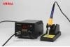
|
Programmable Electrometer
|
The Partial Discharge Detector and Analyser is available at Department of Electrical Engineering, IIT Kanpur. This facility is currently installed in High Voltage Laboratory. Keithley’s 51/2 – digital Model 6517A Electrometer /High Resistance Meter offers high accuracy and sensitivity. With reading rates of up to 125 readings/second, the Model 6517A offers quick, easy way to measure low level currents.
Important features of Electrometer (Model 6517A):
Exceptional sensitivity and accuracy for voltage, current, charge, and V/I resistance and resistivity measurements. Relative humidity and external temperature can be measured.
The internal 1000V V-source can be configured with the ammeter to make V/I resistance/resistivity measurements, and to force voltage, measure current.
Readings and set up data can be stored and recalled from memory. Over 15,000 readings can be stored in the buffer and up to 10 instrument setups can be stored in memory.
Built–in tests for the following applications: device characterisation, resistivity, high resistance/resistivity (alternating polarity method), surface insulation resistance and voltage sweeps.
|
Location:
|
High Voltage Laboratory, Department of Electrical Engineering
IIT Kanpur
|
Contact:
|
Prof. Nandini Gupta
This email address is being protected from spambots. You need JavaScript enabled to view it.
|
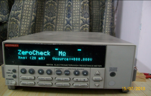
|
Pulsed LASER Deposition Unit
|
Pulsed LASER Deposition is thin film deposition technique in which highly energetic pulsed LASER beam is focused on the target material in presence of vacuum or controlled background gas environment. This causes the vaporization of target material in form of plasma plume which is deposited as thin film on the substrate. Stoichiometry and roughness of the film can be controlled by manipulating LASER parameters, gas pressure inside the chamber and substrate temperature, The unit is comprised of two parts: LASER and deposition chamber.
LASER specifications:
Chamber specifications:
-
Chamber consists of six target holders and one substrate holder for multilayer deposition.
-
Base pressure can be reached up to ~10-7mbar with the help of rotary and turbo molecular pump.
-
Presently highly pure oxygen is used for deposition and the pressure is controlled using mass flow controller with precession of 0.1 mbar.
-
Maximum substrate can be reached up to 750º C.
-
Completely automated deposition process.
|
Location:
|
Department Of Materials Science & Engineering,
IIT Kanpur
|
Contact:
|
Prof. Ashish Garg
This email address is being protected from spambots. You need JavaScript enabled to view it.
Prof. Deepak Gupta
This email address is being protected from spambots. You need JavaScript enabled to view it.
|
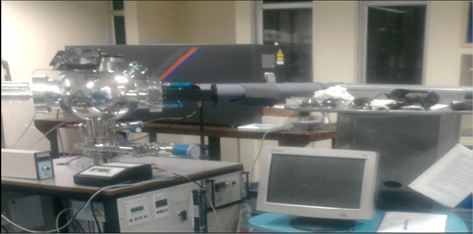
|
|
Phase Doppler Particle Analyzer (PDPA)
|
The Phase Doppler Particle Analyzer (PDPA, see Figure 1) is procured in 2008 at Department of Aerospace Engineering with financial contribution from Department of Science and Technology under FIST scheme.
Unique features:
The Phase Doppler Method is based upon the principles of laser induced light scattering interferometry, (see Figure 2). Measurements are made at a small, non-intrusive optical probe volume defined by the intersection of two laser beams (see Figure 3). As a particle passes through the probe volume, it scatters light from the beams into a multi-detector receiving probe, strategically located at an Off-axis collection angle. The phase shift between the Doppler burst signals from different detectors is proportional to the size of the spherical particles. PDPA system electronics provide accurate and reliable flow velocity and particle size data from all measurement situations - from simple flows to high speed and low SNR situations. Figure 4 presents typical flow velocity histogram.
|
Location:
|
Department of Aerospace Engineering,
IIT Kanpur
|
Contact:
|
Prof. A. Kushari
This email address is being protected from spambots. You need JavaScript enabled to view it.
|
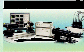
Figure: 1
|
|
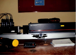
Figure: 2
|
|
Plasma Cleaning System: A TEM sample preparation accessory
|
Procures in the Financial Year: 2011-12Model: Solarus, GatanInc, USA
Entire range of material, metals alloys, ceramics, polymers, composites, electronic as well as biological samples can be studied under various modes of operation of the microscope. But, sample preparation requirement for successful observations is rather stringent and varied depending on the material. The final cleaning of the sample involved organic solvents in many cases. This leaves a contaminant layer of about 5nm on top of the surface of the sample. This layer brings down the quality of images. For conventional imaging this is not deterrent to carrying on the investigation with a compromise on the quality of images. But, when one wants to do HRTEM using the best capability of the microscope and its best resolution, around 0.2nm, this layer becomes a deterrent as the sample thickness at which these studies can be carried out is about 10-20nm (ideal thickness). In this scenario, the contamination layer makes the analysis impossible. The plasma cleaning removes the contamination layer without any damage to the sample surface. This opens up additional scope of investigations and also enable the users to take the full advantage of the high resolution capability of the machine. Another utility of the system is in cleaning up the sample after studying the sample for a specific duration. An intermittent cleaning with plasma removes all contamination and the sample becomes fit again to carry out the studies to its completion.
Elemental analysis with the EDAX system is another situation wherein the plasma cleaning is of great importance. In carrying out the EDS analysis a focused probe of electrons irradiate a sample region of 10-20nm and analyses the X-ray signal generated. During this period of about 50-100 seconds of irradiation, the specific region gets a carbon contamination built up and imaging this area is not possible after EDS analysis. In this sort of situations the plasma cleaning of the sample completely removes the contamination only in about 10-15 minutes.
The Solarus plasma cleaning system that we have at EM facility, MSE has the provision for using it with a range of TEM models as well as for SEM stages. Plasma cleaning system will not only enhance the quality of work but also open up for the complete utilization the TEM capability
|
Significance and advantages:
|
-
Enhanced Imaging capability
-
Improved accuracy when preforming composition microanalysis
-
Longer viewing & acquisition times for EDX and EBSD in a SEM
-
Use of smaller probe size; a “must” for STEM and EELS analysis in a TEM/STEM
|
Location:
|
Western Lab, EM Facility, Room No. 107,
IIT Kanpur
|
Contact:
|
Prof. Gouthama
This email address is being protected from spambots. You need JavaScript enabled to view it.
Mr. G. P. Bajpai
This email address is being protected from spambots. You need JavaScript enabled to view it.
|
User Charges: :
|
No Separate charges. TEM users who use the facility pay a nominal charge for TEM usage.
|
|
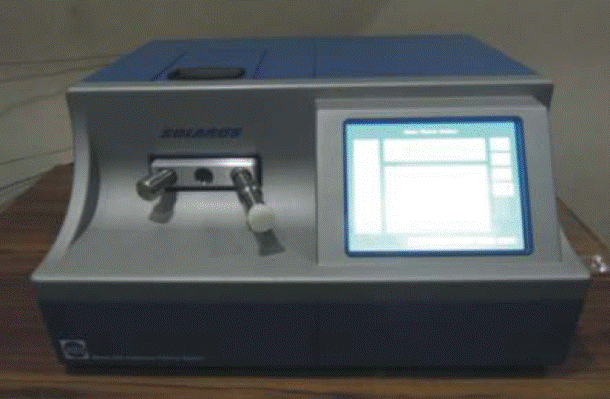
|
Pico Second Pulsed Laser (400nm, 970nm, and 1550nm)
|
-
Pulsed Laser Driver with Repetition rate from single shot to 40 MHz.
-
405nm wavelength Laser Head gives a FWHM Pulse width of 50ps at peak power 588mW (max).
-
971nm wavelength Laser Head gives a FWHM Pulse width of 50ps at peak power 1.25W (max).
-
1550nm wavelength Laser Head gives a FWHM Pulse width of 152ps at peak power 49mW (max).
Other Technical Specifications:
Repetition: frequencies 1, 1/2, 1/4, 1/8, 1/16 of base frequency (Master frequency 40 MHz).
External Trigger Input: Amplitude -5 V to +5 V(max), Trigger level (adjustable) -1 V to +1 V (negative
slope) Required pulse width > 5 ns Delay 35 ± 5 ns (from trigger input to optical output), jitter <40ps Frequency range 10 Hz to 80 MHz Internal impedance 50 Ohms (dynamic), >500 Ohms (static) Connector BNC socket (F)
Synchronization Output: Amplitude < - 800 mV into 50 Ohms (NIM - standard) Pulse width 6ns Delay 12 ns (from falling edge to laser output), jitter < 20 ps Internal impedance 50 Ohms Connector SMA socket (female)
|
Location:
|
Optoelectronics Laboratory (ACES 129) Department of Electrical Engineering,
IIT Kanpur
|
Contact:
|
Prof. Utpal Das
This email address is being protected from spambots. You need JavaScript enabled to view it.
|
Figure 1
|
Figure 2
|
Radian Precision Premier II: Ferroelectric Tester
|
This instrument specializes in characterizing ferroelectric and multiferroic materials for both thin films and bulk structures. Ac electrical characterizations such as P-E, J-E, and polarization fatigue measurements can be performed.
Unique Features:
Measurements:
-
Polarization versus applied field (P-E)
-
Polarization as a function of switching cycle (Fatigue)
-
A.C. current versus voltage (J-E)
Measurement range:
Applied Voltage: 0-99 V (Thin Film) 0-4000 V (Bulk) Temperature: Room Temperature- 120 K Frequency: 1-100 kHz
Data acquisition:
All the above measurements are run on specialized software “Vision”. Run time plodata can be imported to either .txt or .excel formats.
Sample requirement:
Thin film: ferroelectric and multiferroic thin films can be subjected for analysis. Films should contain both bottom and top electrodes.
Bulk: sample should contain both top and bottom electrodes. Sample thickness should be typically less than 1mm.
|
Location:
|
Department Of Materials Science & Engineering,
IIT Kanpur
|
Contact:
|
Prof. Ashish Garg
This email address is being protected from spambots. You need JavaScript enabled to view it.
|
|
RF Analog Signal Generator Facility
|
Radio frequency signal generators (RF signal generators) are a particularly useful item of test equipment widely used in RF design and test applications. E8257D PSG analog signal generator delivers a sufficient level of output power, accuracy, and phase noise performance up to 20 GHz. The PSG analog signal generator's often eliminates the need of an external amplifier for testing high power devices and minimizes test uncertainty to identify errors early in the design process.
Unique features:
Signal Characteristics (250 kHz to 20GHz, 23dbm@20GHz), High SSB phase noise performance, Modulation (AM, FM, ØM, pulse, and scan), 8 ns rise/fall times and 20 ns pulse width, Dual internal function generators (sine, square, triangular), and Step, ramp sweep (frequency and power) etc
|
Location:
|
Microwave Circuit Laboratory, Department of Electrical Engineering,
IIT Kanpur
|
Contact:
|
Prof. Kumar Vaibhav Srivastava
This email address is being protected from spambots. You need JavaScript enabled to view it.
|
|
RF Spectrum Analyzer Facility
|
A spectrum analyzer is a device used to examine the spectral composition of some electrical, acoustic, or optical waveform. It may also measure the power spectrum. We have spectrum analyzer N9320B in Microwave Laboratory of Department of Electrical Engineering that is equipped with the essential functionality. We are using this device to measure the frequency response, noise and distortion characteristics of all kinds of RF circuitry.
Unique features:
Spectrum analysis from 9 kHz to 3 GHz range, minimum non-zero span sweep time (10 ms), RBW (10 Hz to 1 MHz), Built-in power measurements, overall accuracy of ±1.5 db, Sensitivity is -148 dBm DANL with preamplifier, Remote control PC software etc
|
Location:
|
Microwave Circuit Laboratory, Department of Electrical Engineering,
IIT Kanpur
|
Contact:
|
Prof. Kumar Vaibhav Srivastava
This email address is being protected from spambots. You need JavaScript enabled to view it.
|
|
Research Goniometer for Static and Dynamic Light Scattering Analyses
|
In static light scattering, intensity of the scattered light is measured by a detector at different angles. The angle at which the intensity of the light is measured gives the length scale probed by the instrument. In a dynamic light scattering measurement, the time-dependent fluctuations in the scattered light are measured by a fast photon counter. The fluctuations are directly related to the rate of diffusion of the molecule through the solvent. Therefore, the fluctuations can be analyzed to determine a hydrodynamic radius for the sample.
Applications:
1. In the static light scattering mode, time-averaged intensity measurements are made - at either fixed or variable angles - in the range from 8° to 155° and analyzed with software provided for the methods of Zimm, Berry, Debye, Guinier, Kratky etc. Such evaluations using measured angular or concentration dependencies of the intensity of the scattered light provide key information for those interested in the such topics as:
i) Mw Molecular weight determinations
ii) Rg Radius of gyration
iii) A2 Determination of second virial coefficient
iv) Micro-emulsion technology
v) Colloid behavior
vi) Complex fluid characterization
vii) Emulsion polymerization
viii) Particle size growth
ix) Nucleation processes
2. In dynamics light scattering, intensity fluctuations (dynamics) of the scattered light arise from the fact that the scattering particles are undergoing Brownian motion. From these dynamic light scattering measurement many interesting subjects may be explored, among them:
i) Particle size distributions
ii) Particle aggregation phenomena
iii) Micellar systems
iv) Micro-emulsion technology
v) Colloid behavior
vi) Vesicles & lipisomes
vii) Plasmid DNA's
viii) Particle size growth
ix) Nucleation processes & protein crystallization
Cost of the equipment:
USD 63,725
|
Location:
|
Southern Laboratories SL 114, Department of Chemical Engineering
IIT Kanpur
|
Contact:
|
Prof. Yogesh M. Joshi
|
RF Analog Signal Generator Facility
|
Radio frequency signal generators (RF signal generators) are a particularly useful item of test equipment widely used in RF design and test applications. E8257D PSG analog signal generator delivers a sufficient level of output power, accuracy, and phase noise performance up to 20 GHz. The PSG analog signal generator's often eliminates the need of an external amplifier for testing high power devices and minimizes test uncertainty to identify errors early in the design process.
Unique features:
Signal Characteristics (250 kHz to 20GHz, 23dbm@20GHz), High SSB phase noise performance, Modulation (AM, FM, ØM, pulse, and scan), 8 ns rise/fall times and 20 ns pulse width, Dual internal function generators (sine, square, triangular), and Step, ramp sweep (frequency and power) etc.
|
Location:
|
Microwave Circuit Laboratory, Department of Electrical Engineering,
IIT Kanpur
|
Contact:
|
Prof. Kumar Vaibhav Srivastava
This email address is being protected from spambots. You need JavaScript enabled to view it.
|
|
|
Scanning Electron Microscope (SEM)
|
Procured in the Financial Year: 2010-11 Brand - Carl Zeiss
Model Number – EVO18 Special Edition
Capabilities –
-
Very high resolution less than 5nm
-
Magnification up to ONE million times
-
Voltage 1 to 30 KV
-
Variable pressure mode
(For non conducting / Biological samples)
-
Featured with following three detectors
-
SE Mode
-
VPSE Mode
-
CZBSD Mode
Sputter Coater –
Model Number – SC7620 Mini Sputter Coater Quorum Technology
Capabilities –
|
Location:
|
Second floor, Central Facility,
Department of Biological Sciences and Bioengineering (BSBE),
IIT Kanpur
|
Contact:
|
Prof. Dhirendra S. Katti
This email address is being protected from spambots. You need JavaScript enabled to view it.
|
User Charges: :
|
For department (BSBE) users
INR 750/- per slot (90 minutes)
For Institute users (Other than BSBE)
INR 1000/- per slot (90 minutes
For non-IITK users
INR 3500/- per slot (90 minutes)
For Gold coating
INR 250 /- INR per slot for all users
(Service tax is applicable for non-IITK users)
|
|
Scanning Electron Microscope
|
|
|
|
Sputter Coater
|
|
|
Spark Plasma Sintering (SPS)
|
The Spark Plasma Sintering (SPS) facility was established in 2008 at Department of Materials and Metallurgical Engineering with financial contribution from Engineering with financial contribution from Department of Science and Technology and CARE grants of IIT Kanpur. It enables superfast consolidation to make dense ceramics, metals and powder metallurgical materials and is the second one in our country. The facility (Figure 1) is currently installed in the Laboratory for Biomaterials. This facility is used by a number of research groups from various academic institutions/R&D laboratories, including IIT Kharagpur, Naval Materials Research Laboratory, and Vikram Sarabhai Space Center.
Unique features:
SPS is one of the variants of the Field Activated Sintering Technique (FAST). FAST involves the imposition of an electrical field during sintering. A large current (up to 6 kA) is made to flow through a porous powder compact, contained in a graphite die-punch assembly (see Figure 2). This enables to attain high heating rate of up to o600C/min, depending on die size. Typically, holding time of 5-10 minutes at sintering temperature is sufficient to densify the materials in the SPS process and the total processing time is less than one hour.
|
Location:
|
Laboratory for Biomaterials, Department of Materials & Metallurgical Engineering,
IIT Kanpur
|
Contact:
|
Prof. Bikramjit Basu
This email address is being protected from spambots. You need JavaScript enabled to view it.
|
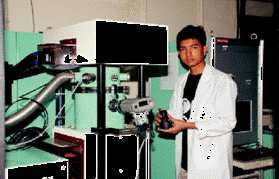
Figure: 1
|
|
Figure: 2
|
|
Figure: 3
|
Spin Coater
|
Spin coating is a procedure used to apply uniform thin films to flat substrates. In short, an excess amount of a solution is placed on the substrate, which is then rotated at high speed in order to spread the fluid by centrifugal force. A machine used for spin coating is called a spin coater, or simply spinner.
|
Location:
|
NET building, Department.of Mechanical Engineering
IIT Kanpur
|
Contact:
|
Prof. Shantanu Bhattacharya
This email address is being protected from spambots. You need JavaScript enabled to view it.
|
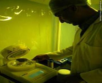
|
Sputtering/PECVD Dual System
|
Sputtering is an important technique of deposition of thin films using Argon and other inert gas plasma created within the right chamber of the shown equipment. The other chamber is a PECVD tool (left chamber which is used to create material films on a substrate. In a PECVD process, gaseous reactants are introduced into a reaction chamber and a plasma is created out of the reactants. Reactions occur on heated substrate surfaces, resulting in deposition of the solid product. Other gaseous reaction products leave the chamber. The gas that carries the reactants is called carrier gas. The PECVD process have a part of their energy delivered by the momentum transfer by the ions in plasma; thus lower substrate temperature is needed, typically of the order of 100-300 deg. C. The PECVD at this time is in need for a Silane system which is very important for feeding the reactants which would react to formulate material films.
|
Location:
|
NET building, Department.of Mechanical Engineering
IIT Kanpur
|
Contact:
|
Prof. Shantanu Bhattacharya
This email address is being protected from spambots. You need JavaScript enabled to view it.
|
|
Small and Wide Angle X-ray Scattering
|
This high-resolution Small- and Wide-Angle X- Ray Scattering (SWAXS) system is particularly designed for real-time, simultaneous small- and wide-angle measurements on powders, liquid crystals and polymeric nanomaterials. The System3 SWAXS Camera basically has the same specifications as the SAXS-system. However, it is equipped with an additional wide-angle x-ray (WAXS) detector covering an angular WAXS range from 18° to 26°. It is powered by an X-ray micro-source that operates at a maximum of 50 Watt electrical power, as compared to the several Kilowatts needed for customary x-ray generators, A compact modular laboratory unit for 2-D SAXS, SWAXS and GISAXS with high brilliance is presented, that facilitates nanostructure analysis of bulk materials, liquid crystals, (bio-) polymer or nanoparticle solutions, and thin solid films. The system, S3-MICRO, is based upon a combination of a point-focus microbeam delivery system (GeniX from Xenocs, Grenoble, France) working at a maximum power of 50 Watt with the Hecus S3-camera architecture with 1-D and 2-D detectors.
|
Location:
|
Thematic Unit of Excellence,
IIT Kanpur
|
Contact:
|
Prof. Ashutosh Sharma
This email address is being protected from spambots. You need JavaScript enabled to view it.
Dr. Prabhat Dwivedi
This email address is being protected from spambots. You need JavaScript enabled to view it.
Dr. Dinesh Deva
This email address is being protected from spambots. You need JavaScript enabled to view it.
|
|
SNOM/Confocal/μRa
|
WITec, alpha 300 series microscope, includes the Confocal Raman Microscope, the Scanning Near-field Optical Microscope (SNOM) and the Atomic Force Microscope in a single integrated unit. Switching between the different modes can easily be done by rotating the objective turret. The alpha SNOM uses unique micro-fabricated SNOM-cantilever sensors for optical microscopy with spatial resolution below the diffraction limit. The micro-Raman represents a new generation imaging systems, focusing on high resolution as well as high speed spectrum and image acquisition. Its sensitive setup allows for the nondestructive imaging of chemical properties without specialized sample preparation. Differences in chemical composition, although completely invisible in the optical image, will be apparent in the Raman image and can be analyzed with a resolution down to 200 nm. The confocal setup reduces unwanted background signals, enhances contrast and provides depth information. Atomic Force Microscope (AFM) modules present in this instrument designed specifically for Materials Research, Nanotechnology, and Life Science. It integrates a scientific-grade optical microscope for superior optical access, easy cantilever alignment, and high resolution sample survey. All standard AFM modes as well as Confocal Microscopy and Confocal Raman Microscopy and SNOM are supported and offer extraordinary opportunities for R&D.
|
Location:
|
Thematic Unit of Excellence,
IIT Kanpur
|
Contact:
|
Prof. Ashutosh Sharma
This email address is being protected from spambots. You need JavaScript enabled to view it.
Dr. Prabhat Dwivedi
This email address is being protected from spambots. You need JavaScript enabled to view it.
Dr. Dinesh Deva
This email address is being protected from spambots. You need JavaScript enabled to view it.
|
|
Scanning Mobility Particles Sizer (SMPS)
|
Counter (CPC). Electrostatic classifier consists of impactor assembly, bipolar charger and differential mobility analyzer(DMA). First poly disperse particles enter through impactor where those larger than cut off size are removed. Then the aerosol particles enter into the Kr-85 bipolar charger, which exposes aerosol particles to bipolar ions. The sheath air and charged particles are introduced at the top of the DMA and both flow down without mixing with each other and by maintaining laminar flow. The DMA consists of two concentric metal cylinders. The inner rod maintains negative voltage and outer cylinder is grounded thus lectric field is generated in annular space of DMA. Positive charged aerosol particles move towards the inner rod through sheath air. The aerosol particles are sized according to their electrical mobility. Nearly mono disperse aerosols then enter into the CPC. Here, the aerosol mixes with butanol vapor, undergoessuper saturation resulting in condensation of vapor on aerosol surface. Consequently, the aerosol particles grow to a size that can be detectable by light scattering.
Technical Specifications:
Impator orifice: 0.0457 cm. 0.0508 cm, 0.0701 cm, Particle Size: Long DMA: 10 -700 nm diameter, Nano DMA: 4 -150 nm. Both the DMAs can run at low and high flow rates (0 .3 and 1.5 lpm) SMPS can measure particles up to 2×10⁸ particles cm-3.
|
Location:
|
Environmental Engineering Laboratory, WL 116
IIT Kanpur
|
Contact:
|
Prof. S. N. Tripathi
This email address is being protected from spambots. You need JavaScript enabled to view it.
|
Figure: 1
|
Servo-Hydraulic Actuators for Load Application
|
Three servo-hydraulic actuators (Make: MTS Systems Corp., USA) have been acquired to enhance the load application capability of the existing Cyclic Testing Facility. One 500kN (Model: 243.45T) was purchased during 2000-01 and two 100kN (Model 244.22) were acquired during 2005-06. These actuators can apply loads in both displacement- and load-controlled mode to simulate various structural loading environment. These are essential loading equipment for simulating loading environment typical for earthquakes; however, they can be used for gravity loads simulation as well.
Technical Specifications:
Force Capacity: +/- 500 kN and +/- 100 kN; Stroke : +/- 125 mm. Swivel Base and Swivel Head. Controller for actuators are capable of applying programmable loading cycles under load, stroke and strain control mode apart from standard sine, ramp, triangle, etc. function for cyclic tests. The actuators are being operated using Hydraulic Power Supply available in the laboratory having the flow capacity of 237lpm at 2.1 MPa.
|
Location:
|
Structural Engineering Laboratory (Workshop – II), Department of Civil and Mechanical Engineering,
IIT Kanpur
|
Contact:
|
Prof. C. V. R. Murty
This email address is being protected from spambots. You need JavaScript enabled to view it.
Prof. Durgesh C. Rai
This email address is being protected from spambots. You need JavaScript enabled to view it.
|
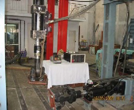
Figure 1
|
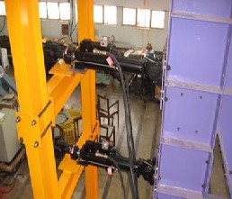
Figure: 2
|
Sorvall MTX 150 Micro-Ultracentrifuge
|
Centrifugation involves the use of centrifugal force, so as to increase the effective gravitational force on the components of a mixture, in order to separate them. The rate of centrifugation of a particle in a mixture is specified by the acceleration applied to the sample measured in revolutions per minute (rpm). The settling velocity of the particle is a function of its size and shape, viscosity of the medium, besides other factors. The ultracentrifuge is optimized for spinning a rotor at very high speeds, capable of generating acceleration as high as 1,000,000 g (9,800 km/s²).These high centrifugal forces are used to isolate very small particles, including ribosomes, proteins, viruses and to study membrane fractionation.
-
Regulatory standards: cCSAus, CE, IEC61010-2-020, EN61326-1 2006
-
Simple operation
-
The Sorvall MTX 150 microultracentrifuge provides user-friendly, reliable operation to simplify rotor loading, instrument setup, and instrument operation. The Sorvall MTX 150 also offers visual tube balancing for enhanced ease of use.
-
Self locking rotor system automatically secures the rotor to the drive shaft. This innovation eliminates the need to manually secure the rotor, facilitation rotor
installation and enhancing safety.
-
GMP/GLP Data compliance and Management
-
The Sorvall MTX 150 offers traceability and quality control for biopharmaceutical processing needs. A USB port allows connectivity to a memory stick, facilitating output of operating data in CSV format.
|
Location:
|
BSBE,
IIT Kanpur
|
Contact:
|
Prof. Jonaki Sen
This email address is being protected from spambots. You need JavaScript enabled to view it.
Prof. A. Bandopadhyay
This email address is being protected from spambots. You need JavaScript enabled to view it.
Prof. Pradip Sinha
This email address is being protected from spambots. You need JavaScript enabled to view it.
|
Sorvall Sure-Spin 630 Ultra Centrifuge Rotor
|
|
Sorvall Sure Spin 630 is a swinging bucket rotor for ultracentrifugation applications. Many procedures like density gradient based separations require a swinging bucket to achieve the best results. This rotor has comparatively long path length and therefore centrifugation can be done for a longer period for better resolution. The Sure-spin 630 swinging bucket rotor is supplied with two interchangeable sets of buckets which can be used for a variety of applications. The 17 and 36 ml buckets are relatively long and skinny, making them ideal for rate zonal runs. The unique top loading design allows the operator to load samples with unprecedented ease.
Applications:
-
Protein interactions
-
Isolation of RNA, Ribosome
-
Isolation of viruses
-
Pelleting protocols for immune complexes, DNA, certain viruses, and subcellular
organelles or glycoproteins
-
Separation of organelles
-
Separation of mRNA, DNA
-
Cell synchronization
-
Protein isolation
-
Nucleic acid isolation
|
Location:
|
Department of Electrical Engineering,
IIT Kanpur
|
Contact:
|
Prof. S. Sundar Kumar Iyer
sskiyer@ iitk.ac.in
|
Figure: 1
|
Sorvall WX100 Floor Ultracentrifuge
|
Centrifugation involves the use of centrifugal force, so as to increase the effective gravitational force on the components of a mixture, in order to separate them. The rate of centrifugation of a particle in a mixture is specified by the acceleration applied to the sample measured in revolutions per minute (rpm). The settling velocity of the particle is a function of its size and shape, viscosity of the medium, besides other factors. The ultracentrifuge is optimized for spinning a rotor at very high speeds, capable of generating acceleration as high as 1,000,000 g (9,800 km/s²).These high centrifugal forces are used to isolate very small particles, including ribosomes, proteins, viruses and to study membrane fractionation.
|
|
Location:
|
BSBE,
IIT Kanpur
|
|
Contact:
|
Prof. Jonaki Sen
This email address is being protected from spambots. You need JavaScript enabled to view it.
Prof. A. Bandopadhyay
This email address is being protected from spambots. You need JavaScript enabled to view it.
Prof. Pradip Sinha
This email address is being protected from spambots. You need JavaScript enabled to view it.
|
Thin-film Thickness Measurement System
|
Thickness and optical constants (n and k) are measured quickly and easily with the F20 advanced spectrometry system. Spectral analysis of reflectance from the top and bottom of the thin film provides thickness, refractive index, and extinction coefficient in less than a second. Virtually any smooth, translucent, or lightly absorbing film may be measured, including SiO2, SiNX, DLC, Photoresists, Polymer layers, Polyimide, Polysilicon, Amorphous Silicon, Silicon, Parylene and Industrial Coatings. For thickness measurements, all that is required in most cases is a smooth, reflective substrate. For optical constant measurements, a flat specularly reflecting substrate is required. If the substrate is transparent, the backside of the substrate must be prepared so that it is not reflective. Examples include: Silicon, Glass, Aluminum, GaAs, Steel, Polycarbonate, Polymer films etc. For measurements on patterned surfaces and other applications that require a spot size as small as 10 microns, just add the model F40 to the microscope. For common microscopes the F40 is a simple bolt-on attachment, complete with a c-mount for a CCD camera.
|
Location:
|
Thematic Unit of Excellence,
IIT Kanpur
|
Contact:
|
Prof. Ashutosh Sharma
This email address is being protected from spambots. You need JavaScript enabled to view it.
Dr. Prabhat Dwivedi
This email address is being protected from spambots. You need JavaScript enabled to view it.
Dr. Dinesh Deva
This email address is being protected from spambots. You need JavaScript enabled to view it.
|
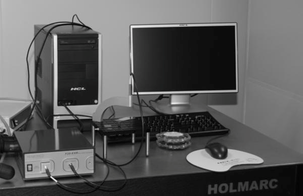
Figure: 1
|
Thermal Cycler (PCR Machine)
|
The Thermal Cycler (also known as a Thermocycler, PCR Machine or DNA Amplifier) is a laboratory apparatus used to amplify segments of DNA via the Polymerase Chain Reaction (PCR). The device has a thermal block with holes where tubes holding the PCR reaction mixtures can be inserted. The cycler then raises and lowers the temperature of the block in discrete, pre-programmed steps.
It is an important instrument which is needed in all the labs working in the field of gene cloning. A basic PCR set up requires several components and reagents. These components include:
-
DNA template that contains the DNA region (target) to be amplified.
-
Two primers, which are complementary to the DNA regions at the 5' (five prime) or 3' (three prime) ends of the DNA region.
-
A thermostable DNA polymerase such as Taq polymerase .
-
Deoxynucleoside triphosphates (dNTPs), the building blocks from which the DNA polymerases synthesizes a new DNA strand.
-
Buffer solution, providing a suitable chemical environment for optimum activity and stability of the DNA polymerase.
-
Divalent cations, magnesium or manganese ions; generally Mg2+ is used Monovalent cation potassium ions.
Unique Features:
There are many companies making Thermocyclers such as BioRad, Thermo, Eppendorf, having the basic set-up with some specific features:
The Eppendorf Mastercycler personal is a high quality, compact thermal cycler. In addition to its speed and precise block homogeneity, it offers first-rate operational flexibility. Its universal block with a 25-well format can accommodate 25 x 0.2 ml tubes,16 x 0.5 ml tubes or microtiter plates in a 5 x 5 grid format.
The Eppendorf Mastercycler® Personal is an essential instrument of our lab. For the last six years, it is being used for regular PCR of the DNA for cloning purpose. Apart from our lab, it is available to everyone in the institute for the use. The various reagents and buffers required for the PCR reactions have to be brought by the person using it.
|
Location:
|
Department of Chemistry,
IIT Kanpur
|
Contact:
|
Prof. Gurunath R.
This email address is being protected from spambots. You need JavaScript enabled to view it.
|
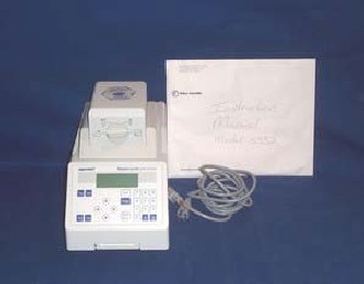
Figure: 1
|
Thermal Evaporation (Thin-film Deposition) system
|
The Thermal Evaporator system purchased from Consolidated Vacuum Corporation, New York, can deposit almost all metals onto various substrates by boiling the metal and evaporating it at high vacuum. The bell-jar connected to a diffusion vacuum pump gets evacuated to 1x10⁻⁶ mbar. The metal to be deposited is placed in a molybdenum/tungsten boat and heated. The evaporated metal vapor gets adhered / deposited onto the substrate placed over the boat. The attached HHV Thickness Monitor can measure accurately the thickness of the deposited film from 10 nm to 10 μm. This is an in-house facility and cannot be borrowed out of the Lab. Use On Payment basis - for details see Forms in http://www.iitk.ac.in/ibc/
|
Location:
|
Ion Beam Complex, NL-105, Department of Physics, IIT Kanpur.
|
Contact:
|
Co-ordinator, IBCOR
Mr. S. Krishnasamy
Technical Superintendent, IBC
(
This email address is being protected from spambots. You need JavaScript enabled to view it.
).
Phone: 7986 / 6993
|
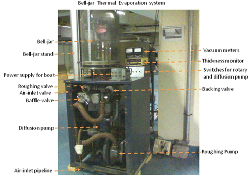
Figure: 1
|
UV-Vis Spectrophotometer
|
Ultraviolet-visible spectroscopy or ultraviolet-visible spectrophotometry (UV-Vis or UV/Vis) refers to absorption spectroscopy in the ultraviolet-visible spectral region. This means it uses light in the visible and adjacent (near-UV and near-infrared (NIR)) ranges. UV/Vis spectrophotometer is used in the quantitative determination of concentrations of the absorber in the solutions of transition metal ions and highly conjugated organic compounds. The UV-Vis Spectrophotometer (Varian Cary 100) (Figure 1) was established in the Core Lab in the Core Lab (201D) in 2007 with the DRDO grant of the Institute.
Basic Principle:
The Beer-Lambert law states that the absorbance of a solution is directly proportional to the concentration of the absorbing species in the solution and the path length (Figure 2). Thus, for a fixed path length, UV/Vis spectroscopy can be used to determine the concentration of the absorber in a solution. The absorbance changes with concentration. This can be taken from references (tables of molar extinction coefficients), or more accurately, determined from a calibration curve.
Unique Features:
Quartz overcoating protects the optics from the environment and allows cleaning without damage to their reflective surface. Sealed optics prevents exposure to corrosive environments. Double choppers ensure that the sample and reference beam strike the detector at the same point, removing any errors due to non uniformity of the detector. Variable slits allow optimum control over data resolution. The spectral bandwidth can be set down to 0.2 nm. A phase locked wavelength drive prevents peak shifts and peak suppression at high scan speeds. The large sample compartment gives more flexibility in sample size.
|
Location:
|
Department of Chemical Engineering,NL Lab,
IIT Kanpur
|
Contact:
|
Prof. Nishith Verma
This email address is being protected from spambots. You need JavaScript enabled to view it.
|
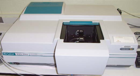
Figure 1
|
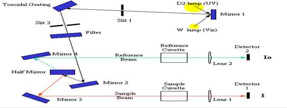
Figure 2
|
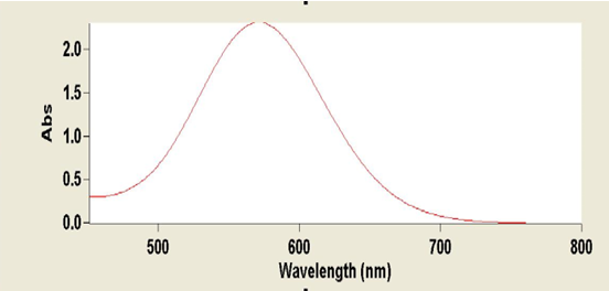
Figure: 3
|
Upgradation for Raman System
|
The micro-Raman facility consists of a 5watt Argon-ionlaser, triplemate spectrometer system (1877E), PMT and liquid nitrogen cooled CCD detectors, all of which interfaced to a computer (System is almost 20 years old). The upgradation of the data acquisition system to the present state of interfacing with Pentium 4 computer, a new CCD controller and PMT high voltage supply have been obtained through the CARE grant.
Technical Specifications:
-
Two Spex 232/488 Retro RS232 and IEEE-4888 two way interface. RS232 is a 25 pin Standard Rs-232 null modem cable that is connected to spectrometer controller to the computer.
-
SAQ-302DPM, SpectrAcq2 Data Acquisition System: Gain Range 1,10,100 and 1000 X, Input voltage range +\-10, 1, 0.1, 0.01Volts, Maximum signal 10micro Amps/10 Volts, ADC resolution 16 Bits, Voltage supply +\-15V.
-
PMT-HVPS, Stand alone high voltage Power Supply: Output Voltage 0 to -2000V DC, maximum output current 1mA, ripple noise 30mV peak to peak, input line voltage 24V DC.
-
Labspec windows based software along with Pentium 4 PC: Computer with 256 MB of RAM, 80GB Hard disk with Pentium 4 processor with a Labspec windows based software to control Raman System.
-
One Nitrogen cooled CCD: Typical sensor operating temperature -133 oC, optical distance from sensor to front flange 0.791mm.
|
Location:
|
Biomedical Optics and Spectroscopy Laboratory, Sl-111, Department of Physics,
IIT Kanpur
|
Contact:
|
Dr. Asima Pradhan
This email address is being protected from spambots. You need JavaScript enabled to view it.
|
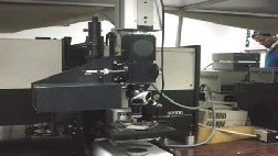
Figure: 1
|
Vacuum Induction Melting Unit
|
Induction heating is a process wherein induced eddy currents heat conductive materials. This heating can be used to melt metals and make alloys. Vacuum Induction melting offers an attractive combination of a controlled atmosphere (vacuum or inert gas) and precise control on the melting process. The induction melting facility (Figure 1) was established in the Symmetry Lab (WL-207, Materials Science and Engineering) in 2009 with initiation and special grants from the Institute.
Unique Features:
Depending on the inductive coupling of the coil with the charge materials, the induction furnace can go to a temperature of 1800ºC or more. About 100 g of metals can be melted at a time. There are three main parts to the system: chiller, power unit and vacuum unit. The vacuum unit with rotary and diffusion pumps can attain a vacuum of 106 m bar. The power can deliver a maximum power of 15 kW.
|
Location:
|
Symmetry Lab (WL-207),
Department of Materials Science and Engineering,
IIT Kanpur
|
Contact:
|
Prof. Anandh Subramaniam,
This email address is being protected from spambots. You need JavaScript enabled to view it.
|
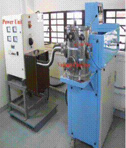
Figure: 1
|
|
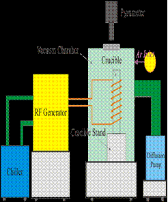
Figure: 2
|
Vacuum annealing system [up to 1000℃]
|
The vacuum annealing system comprises of a cylindrical furnace with an Alumina tube of diameter 1.5” and length 12”, maintaining a PID controlled temperature from 120℃ to 1000℃. The solid sample to be vacuum annealed is placed in a quartz tube of diameter 1.2” and evacuated to 1x10⁻⁶ mbar using a turbo-molecular pump, and then the quartz tube is inserted into the furnace for the desired annealing period. This is an in-house facility and cannot be borrowed out of the Lab. Use On Payment basis - for details see Forms in http://www.iitk.ac.in/ibc/
|
Location:
|
Ion Beam Complex, NL-105, Department of Physics, IIT Kanpur.
|
Contact:
|
Co-ordinator, IBCOR
Mr. S. Krishnasamy
Technical Superintendent, IBC
(
This email address is being protected from spambots. You need JavaScript enabled to view it.
).
Phone: 7986 / 6993
|
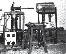
|
VECTOR NETWORK ANALYZER FACILITY
|
A Network Analyzer is an instrument that measures the network parameters of electrical networks. Network Analyzers commonly measure S-parameters because reflection and transmission of electrical networks are easy to measure at high frequencies. Network analyzers are often used to characterize two-port active and passive devices, but they can also be used on networks with an arbitrary number of ports. Vector error correction, which improves measurement accuracy by removing the effects of inherent measurement-system errors, requires both magnitude and phase data to build an effective error model. Phase-measurement capability is very important even for scalar measurements such as return loss, in order to achieve a high level of accuracy
Unique Features:
N5230A PNA-L Network Analyzer is one of the variants of the Vector Network Analyzer (VNA). It works in the frequency range of 10 MHz – 50 GHz. Its dynamic range is 108 dB. This Network Analyzer offers OSL/TRL calibration and waveguide measurements.
|
Location:
|
Microwave Circuit Laboratory, Department of Electrical Engineering,
IIT Kanpur
|
Contact:
|
Prof. Kumar Vaibhav Srivastava
This email address is being protected from spambots. You need JavaScript enabled to view it.
|
Figure: 1
|
Visual Control Set Up
|
This experimental setup consists of a seven degrees of freedom manipulator from Schunk, Germany and a six degrees of freedom manipulator from ABB and stereo vision system. Experiments in visual control, trajectory tracking, real-time optimal redundancy resolution and cooperative, manipulation are being performed. This experimental setup is unique in the national scenario. This facility has been created through FIST, DST and MHRD sponsored projects.
One Patrolbot and Two Pioneers from Active Media Robotics
These facilities are being used for experiments in visual navigation, visual tracking of rigid and non-rigid objects, multi-robot system control and coordination. These facilities have been developed through FIST and DRDO sponsored projects
|
Location:
|
Intelligent Systems Laboratory, Department of Electrical Engineering,
IIT Kanpur
|
Contact:
|
Prof. Laxmidhar Behera
This email address is being protected from spambots. You need JavaScript enabled to view it.
|
Figure: 1
|
Figure: 2
|
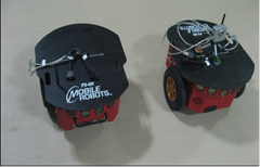
Figure: 3
|
Virtually-Instrumented Polymerization Reactor with on-line Optimal Control Facility
|
In the virtually instrumented, 1-liter Parr reactor set-up, the temperature and power-input to a constant speed agitator motor, are measured/recorded continuously as the polymerization (of methyl-methacrylate; MMA) takes place. The polymerization can be carried out at almost any desired set-point temperature history. The ‘state’ of the system (namely, the monomer conversion and the weight-average molecular weight) can be estimated on-line using the soft-sensors developed in the lab. On-line model adaptation and on-line optimal control for this system have also been carried out.Other systems can be/are being studied.
Technical Specifications:
1 liter SS Parr reactor with magnetic stirrer and motor-speed control, and relevant virtual instrumentation units.
|
Location:
|
Northern Lab-II, Room 302 Department of Chemistry,
IIT Kanpur
|
Contact:
|
Prof. Santosh K. Gupta
This email address is being protected from spambots. You need JavaScript enabled to view it.
|
Figure: 1
|
Wire Bonder
|
Wire bonding is a method of making interconnections between a microchip and other electronics as part of semiconductor device fabrication.
|
Location:
|
NET building, Department.of Mechanical Engineering
IIT Kanpur
|
Contact:
|
Prof. Shantanu Bhattacharya
This email address is being protected from spambots. You need JavaScript enabled to view it.
|
Figure: 1
|
Zeta Potential and Submicron Particle Size Analyzer
|
The Delsa Nano series is a new generation of instruments that use photon correlation spectroscopy (PCS), which determines particle size by measuring the rate of fluctuations in laser light intensity scattered by particles as they diffuse through a fluid, for size analysis measurements and/or electrophoretic light scattering (ELS), which determines electrophoretic movement of charged particles under an applied electric field from the Doppler shift of scattered light, for zeta potential determination. This series has a broad range of capabilities, including conventional static and automatic titration measurements for both size and zeta potential distributions of suspended particles in a wide range of size and concentration. The Delsa Nano C also can measure zeta potential of a solid surface or film..
|
Location:
|
Thematic Unit of Excellence,
IIT Kanpur
|
Contact:
|
Prof. Ashutosh Sharma
This email address is being protected from spambots. You need JavaScript enabled to view it.
Dr. Prabhat Dwivedi
This email address is being protected from spambots. You need JavaScript enabled to view it.
Dr. Dinesh Deva
This email address is being protected from spambots. You need JavaScript enabled to view it.
|
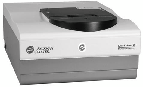
Figure: 1
|
ZSX Primus II Wave length Dispersive X-Ray Fluorescence Spectrometer
|
XRF is used to determine chemical composition of all kinds of materials. The materials can be in solid, liquid, powder, filtered or other form. The method is fast, accurate and non-destructive, and usually requires only a minimum of sample preparation. Applications are very broad and include the metal, cement, oil, polymer, plastics, and food industries, along with mining, mineralogy and geology, and environmental analysis of water and waste materials.
In XRF, X-Rays produced by irradiate the sample. In most of the cases, the source is an X-rays tube but alternatively it could be synchrotron or a radioactive material. The elements present in the sample will emit fluorescent X-ray radiation with discrete energies that are characteristics for these elements. A different energy is equivalent to a different color. By measuring the energies of the radiation emitted by the sample it is possible to determine which elements are present. This step is called Qualitative analysis. By measuring the intensities of the emitted energies it is possible to determine how much of each element is present in the sample. This step is called Quantitative Analysis.
Our WD-XRF system can detect elements from Na to U. The concentration range goes from ppm levels to 100%. Generally speaking, elements with high atomic numbers have better detection limits than lighter elements.
Specification
X-ray Spectrometer assembly tube consisting of: X-ray generator 4kW , 60kV-150mA
Primary beam filters with Al25, Ti20, Cu25, Zr150
6 position diaphragm
(35, 30, 20, 10, 1, 0.5mm φ)
Divergence Slit : 3 positions
Receiving Slit : For SC , for F-PC
Goniometer
Angular Ranges for detectors : SC: 5˚ -118˚ , F-PC 13˚ -148˚
Max Scan Speed : 1400˚ /Min ( 2 )
Angular Reproducibility : + 0.0005˚
Continues Scan : 0.1 – 240 ˚ / Min
Detector : For heavy elements SC , Counting linearity : 1000kcps
Detector: For light elements F-PC, Counting linearity : 2000kcps
Attenuator : IN – OUT Automatic Exchange ( Attenuation 1/10)
3 position slit changer with coarse and fine slit
Windows XP Software with SQX including Library
|
Location:
|
X-Ray Fluorescence Laboratory Room No. 101, ACMS Building
IIT Kanpur
|
Contact:
|
Prof. Debajyoti Paul
This email address is being protected from spambots. You need JavaScript enabled to view it.
|
User Charges: :
|
IIT Kanpur users
INR. 1000 per sample (10 Major element oxides & 20 selected trace elements)
Outside IITK users
INR. 1200 per sample (10 Major element oxides & 20 selected trace elements)
Industry & Consultancy Work
INR. 2000 per sample (10 Major element oxides & 20 selected trace elements)
(Service tax is applicable for non-IITK users)
|
|
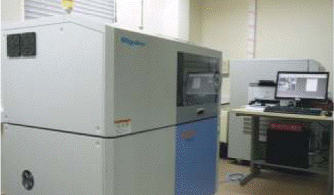
Figure: 1
|
|
|
 |