|
Spark Plasma Sintering (SPS) |
||||
|
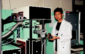
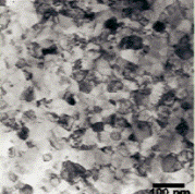
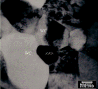
Unique features:SPS is one of the variants of the Field Activated Sintering Technique (FAST). FAST involves the imposition of an electrical field during sintering. A large current (up to 6 kA) is made to flow through a porous powder compact, contained in a graphite die-punch assembly (see Figure 2). This enables to attain high heating rate of up to o600C/min, depending on die size. Typically, holding time of 5-10 minutes at sintering temperature is sufficient to densify the materials in the SPS process and the total processing time is less than one hour. |
||||
|
Location: |
||||
|
Laboratory for Biomaterials, Department of Materials & Metallurgical Engineering, |
||||
|
Contact: |
||||
|
Prof. Bikramjit Basu This email address is being protected from spambots. You need JavaScript enabled to view it. |
||||
|
|
||||
 |
||||
 |
||||