
Scanning Electron Microscopy Facility
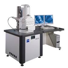
About instrument (Carl Zeiss EVO 50)
Scanning Electron Microscope is a versatile analytical microscope with a large specimen chamber and can handle large specimens at the analytical working distance of 8.5mm owing to a combination of the inclined detectors and the sharp conical objective lens.
ENERGY DISPERSIVE X-RAY MICROANALYSIS
Microstructures at SEM can be analyzed for its elemental composition in more detail using EDX system. This is a non-destructive analysis and the elements and their concentration in the sample can be determined reasonably accurately. EDS (EDX) Analysis provides elemental/Phase composition analysis of a sample inside a SEM. Also microstructural analysis i.e. EBSD (Electron BackScatter Diffraction Analysis) can be done to characterize grain structures. INCA and AZtec from Oxford is a new and revolutionary materials characterization system that gathers accurate data at the micro- and nanoscales
Essential Specification: EVO 50
Resolution |
2.0nm@ 30kV |
Acceleration Voltage |
0.2 to 30 kV |
Magnification |
5x to 1,000,000x |
Field of View |
8.5 mm at the Analytical Working Distance (AWD) |
X-ray Analysis |
8.5 mm AWD and 35° take-off angle |
Detectors |
SE in HV - Everhart-Thornley BSD in all modes - quadrant semiconductor diode |
Some salient features of EDX analysis of known or unknown materials
- Qualitative and quantitative analysis for all elements from carbon upwards in the periodic table
- Quantitative analysis of homogenous bulk materials having features = 2 µm
- Qualitative analysis of features = 0.2 µm
- Detection limits typically 0.1 – 100 Wt% for most elements
- Multi-element X-ray mapping and line scans Particle analysis – Detection, analysis, morphology and size.
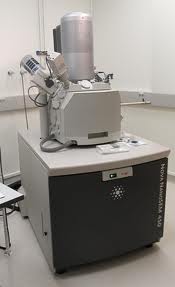
About instrument (Nova NanoSEM 450)
The Nova NanoSEM is a field-emission scanning electron microscope (FE-SEM), which attains ultra-high imaging resolution. The NanoSEM Schottky field-emission source allows the user to achieve high imaging resolution at a range of 0.2-30 kV, at both low (high-resolution imaging) and high (micro analytical imaging) currents. Secondary electron (SE) imaging can be undertaken in both field-free and immersion mode for comprehensive low-to-high resolution imaging of a variety of samples. The Nova NanoSEM is configured with a Bruker SDD-EDS detector and can be manually fitted with a backscattered electron detector for the convenient visualization of compositional differences across the specimen surface
Resolution |
1.0nm@ 30kV |
Acceleration Voltage |
0.2 to 30 kV |
| Magnification |
5x to 1,000,000x with HR/UHR Mode |
Field of View |
5.0 mm at the Analytical Working Distance (AWD) |
X-ray Analysis |
5.0 mm AWD and 35° take-off angle |
Detectors |
In-lens SE detector (TLD-SE) In-lens BSE detector (TLD-BSE) Everhardt-Thornley SED Low vacuum SED (LVD) High sensitivity low kV Directional Backscattered Detector (DBS), BSD in all modes - quadrant semiconductor diode |
Contact Details
Convener: Prof. K. Balani (kbalani@iitk.ac.in) |
Internal: 6194 |
Staff Incharge: Samata Samal (samata@iitk.ac.in) |
Internal: 6053 |
Technical Staff: Mr. Ajay Pratap Singh (ajayps@iitk.ac.in) |
Internal: 6053 |
Technical Staff: Mr. Govind (govindb@iitk.ac.in) |
Internal: 6053 |
Technical Staff: Mr. Surya Prakash Sonkar (spsonkar@iitk.ac.in) |
Internal: 6053 |
Location
Direction (CARL ZEISS EVO 50): click here for navigationDirection (NOVA NANOSEM 450): click here for navigation