|
PCB CAD System |
||||
|
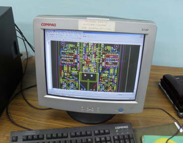
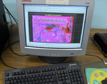
The software used in PCB lab. is Altium. Altium 2009 was procured for designing and fabricating the PCBs. We are using it, becuase it is a powerful tool in designing PCB layout. It has enhanced features like improved interactive routing, user selectable track width, internal routing loops, PCB routing completion detector, preserving track angles while dragging, designing bottom layer layout (mirror has to done) just by flip and editing the board etc. |
||||
|
Location: |
||||
|
PCB Fabrication Laboratory, of Electrical Engineering, |
||||
|
Contact: |
||||
|
Prof. Shyama Prasad Das This email address is being protected from spambots. You need JavaScript enabled to view it. |
||||
|
|
||||
|
|
||||